当前位置:网站首页>Ad9 tips
Ad9 tips
2022-06-23 04:46:00 【Boundless also initial heart】
AD Shortcut key :
SHIFT+S : Single layer display
SHIFT+C :Clear
T S: Select a component corresponding to the schematic diagram pcb components and parts
T M Cancel pcb Check error for
X Mirror image
L Flip to the other side
Altium Designer Summer 09 in draw PCB appear collision Warning How to deal with it ?
This warning should mean that the original is too close , I've been there , It's like the software treats the cylinder as the square . My solution is this : edit PCB original script , Place device body , Place the appropriate shape according to the shape of the original ( It could be a cylinder ), It will be much better after editing the device body .
If you are sure that your drawing is OK , You can also ignore warnings directly : Tools -> Reset error flag , Shortcut key :T M, But this may not lead to errors .
Questioning :
It would be nice if you could set and cancel this warning separately ~~~~
Chase and answer :
Try this : Design -> The rules ->Placement->ComponentClearance, Remove the tick
Powet Plane Connect( Power layer connection type rules )
The power layer connection type rule is used to set which pad type the component pin is connected to the power layer . The dialog box is shown in the figure 5-53 Shown .
This setting is mostly used in multilayer boards , It is mainly used to set the internal power supply and vias belonging to the power supply and ground network in the formation , And the connection mode between the pad and the copper foil .
stay Constraints( Limit ) In the bar , There is a copper-clad model of the power supply layer . There is a drop-down list box in the upper left corner of the model , It is used to set the way in which the component pad is connected to the copper clad , Pictured 5-54 Shown .
Relief connections: Radial connection , That is to say, several wires protruding from the component pad are connected to the copper clad , In this way, the heat transfer between the copper clad area and the pad is relatively slow , During welding, it will not cause poor fusion between the pad and solder due to too fast heat dissipation in the copper clad area .
Direct connections: Direct connection , This connection directly covers the component pad with copper . The advantage of this connection is that the resistance between the pad and the copper-clad area is relatively small , But welding is troublesome .
No Connect: No connection mode , That is, there is no connection between the component and the power layer . This form is not generally used . If you choose Relief connections The way , You also need to set some parameters :
1 Conductor Width: Set the width of the connector .
2 Conductors: Set the number of connecting lines . The alternatives are 2 Root and 4 root .
3 Air-Gap: Set the width of the air gap .
4 Expansion. Set the width between pads and holes .
Select the other two methods without setting these parameters .
In this case , We choose Relief connections( Radial connection ) The way , Set up Conductor Width( The width of the connecting line ) by 10mil,Conductors( Number of connecting lines ) by 4 individual ,Air-Gap( Air gap width ),10mil,Expansion( Width between pad and hole ) by 10mil.
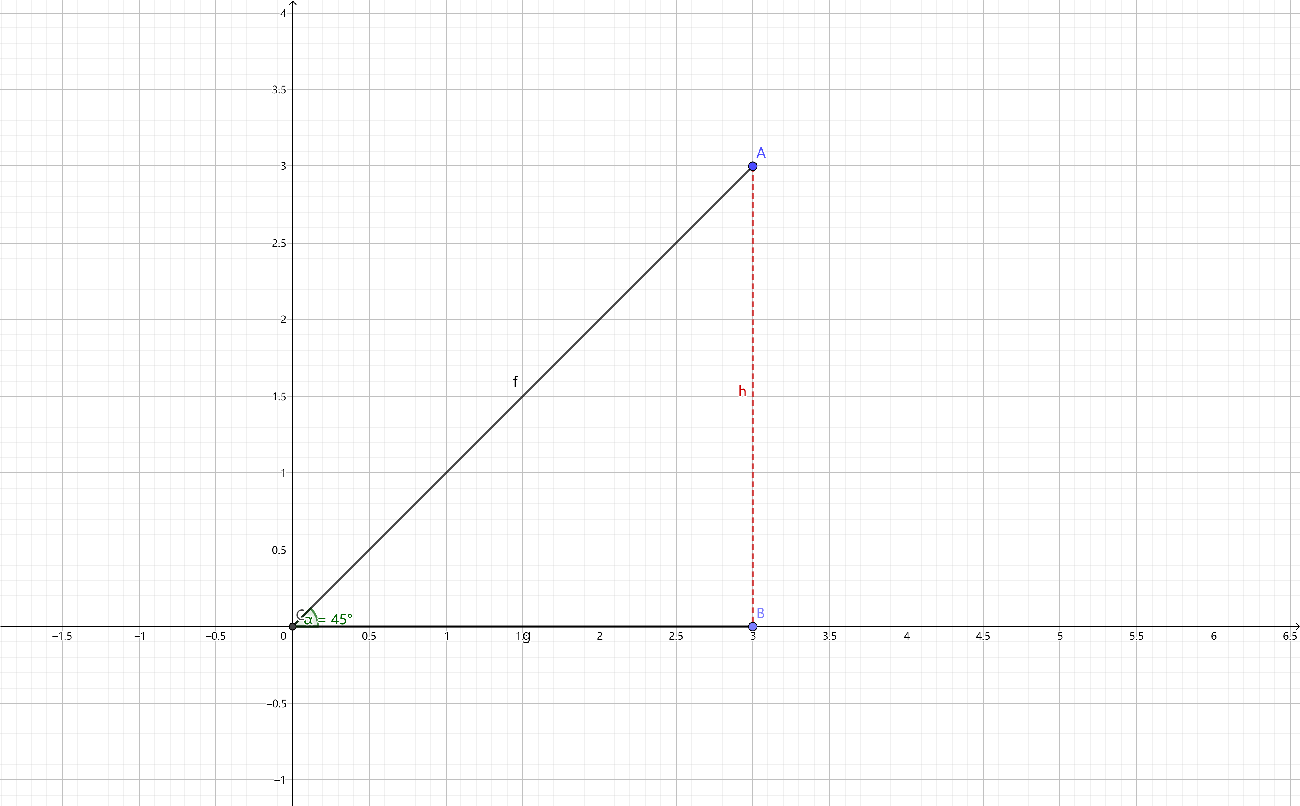
stay AD How to place components obliquely in 45 Degree angle .
45
Or in tools-preferences Under the options-other-rotation The value in is changed to 45 As well as .
边栏推荐
- Does the network disk also roll inside?
- 如何让社交媒体成为跨境电商驱动力?这款独立站工具不能错过!
- Kail 渗透基本素养 基础命令
- 1183. 电力
- 如何解决独立站多渠道客户沟通难题?这款跨境电商插件一定要知道!
- 20000 words + 20 pictures | details of nine data types and application scenarios of redis
- #18生成器函数的参数传递
- 在Pycharm中对字典的键值作更新时提示“This dictionary creation could be rewritten as a dictionary literal ”的解决方法
- Pta:7-61 teacher student information management
- Kali 安装之腾讯云经验遇到坑
猜你喜欢

LabVIEW在同一表中同时显示十六进制字符和普通字符

mysql json

大一学生课设c——服装管理系统

离线数仓建模中常见的概念-术语
Distance measure - cosine distance

国家药品不良反应监测中心 ADR 电子传输EDI解决方案
在Pycharm中使用append()方法对列表添加元素时提示“This list creation could be rewritten as a list literal“的解决方法

JVM调优简要思想及简单案例-为什么需要JVM调优?
Laravel中使用 Editor.md 上传图片如何处理?

Please use the NLTK Downloader to obtain the resource

随机推荐
Principle of 8-bit full adder
altium designer 09丝印靠近焊盘显示绿色警告,如何阻止其报警?
STL教程3-异常机制
After the exception is thrown, the @transactional does not take effect
const理解之二
离线数仓建模中常见的概念-术语
Laravel中使用 Editor.md 上传图片如何处理?
抖音x-bogus和_signature参数分析
距离度量 —— 余弦距离(Cosine Distance)
gson TypeAdapter 适配器
Alkylation process test questions and simulation test in 2022
Notes on writing questions in C language -- free falling ball
[pytoch] calculate the derivative of sin (x) by automatic differentiation
如何解决独立站多渠道客户沟通难题?这款跨境电商插件一定要知道!
#18生成器函数的参数传递
Common interview questions in automated testing
thinkphp6 模版替换
X24cxx series EEPROM chip C language universal reading and writing program
volatile 与线程的那些事
FreeModBus解析1