当前位置:网站首页>Group planning - General Review
Group planning - General Review
2022-06-24 11:36:00 【Schwertlilien】
Always review
Preface
The knowledge points recorded in it are basically within the scope of the examination , There are many knowledge points that have not been written . Examination oriented .
It is suggested that you eat with exercises .
The subject is indeed the one who has passed the exam , But the mark is not very complete . Then the more , Express I I think it is important .

List of articles
- Always review
- Preface
- ( One ) The introduction
- ( Two ) Data representation in a computer
- ( 3、 ... and ) Arithmetic method and arithmetic unit
- ( Four ) Instruction system and assembly language
- ( 5、 ... and ) The storage system
- ( 6、 ... and ) Processor design
( One ) The introduction
1. The development of computers
Of modern computers Theoretical basis : Boolean algebra 、 Material basis : Bistable trigger .
1946 year , The United States ,ENIAC, Electronic digital integration and computers
1946 year 6 month , feng · Neumann proposed to use binary , The core idea of program storage and program control , It has laid the foundation of modern electronic digital computer architecture .
- 1946-1954 year , The first 1 generation , Electronic tube computer ,ENIAC、IBM 701
- 1955-1964 year , The first 2 generation , Transistor computer ,IBM 7030、Univac LARC
- 1965-1974 year , The first 3 generation , Integrated circuit computer ,IBM 360、370、DEC PDP-8
- 1975-1990 year , The first 4 generation , VLSI computer ,IBM 3090、VAX 9000、PC machine 、 Apple machine
- 1991-, The first 5 generation , Multicore processor (4 Nuclear and 8 nucleus )
2. The basic composition of a computer

This is last year's exam !!!
feng · The hardware of Neumann machine is fixed , Different operation functions are realized by programs stored in memory in advance , This is the basic principle of stored program control , It is also the key to distinguish other computing tools .

Computer software :
- Computer language : machine language 、 assembly language 、 High-level language
- Software classification : Systems software 、 Application software 、 middleware
3. The hierarchy of computers

4. The classification of computers
Classified by size and function :
Supercomputers 、 The mainframe 、 medium-size computer 、 minicomputer 、 microcomputer 、 Single chip microcomputer
By use :
Universal machine ( Such as :PC machine )、 Special machine ( Such as : Embedded computers )
According to the characteristics of information processing :(FLYNN) Felling classification
- Single instruction stream single data stream computer (SISD)
- Single instruction stream multi data stream computer (SIMD)
- Multiple instruction stream single data stream computer (MISD)
- Multi instruction stream multi data stream computer (MIMD)
Flynn classification : Classified according to the characteristics of information flow in the process of computer program execution .

5. Computer performance description
( Personally, I think the probability may be a problem )
- MIPS: Millions of instructions executed per second
- MFLOPS: The number of millions of floating-point operations performed per second
- CPI: The number of clocks used to execute each instruction
- N: The number of clocks used to execute each instruction
- f C L K f_{CLK} fCLK: clock frequency


( Two ) Data representation in a computer


1. Comparison of different codes
- True value is + : Original code 、 Complement code 、 The representation of inverse code is the same .
- True value is - : Original code 、 Complement code 、 The representation of inverse code is different .
- Special code shift : 0 Indicates that the true value is negative ; 1 Indicates that the truth value is a positive number .
0 There's a unique code : Complement code 、 Shift the code .
Original code :1000 0000 | 0000 0000
Inverse code :1111 1111 | 0000 0000
The sign bit uses 0 Express positive 、 use 1 Negative : Original code 、 Inverse code 、 Complement code
Shift the code :1 Express positive 、0 Negative
If the truth value is large, the code value is large : Shift the code
The highest symbol bit 1 It's a negative number ( The truth is small, the code is small ): Original code 、 Inverse code 、 Complement code
The larger the true value with negative value, the smaller the code value : Original code
【-1】 repair =【1000 0001】 repair =【1111 1111】 It can be seen that : The largest negative value 、 Maximum code value .
Inverse code = Complement code - 1、 Shift the code = The highest sign bit of complement is reversed So none of them are .
The code value of a negative number is greater than that of a positive number : Original code 、 Inverse code 、 Complement code
The principle is : The highest sign bit of the code value of a negative number is 1
2. Floating point numbers
Normalization means that the absolute value of mantissa is limited to $\frac{1}{2} ~ 1$ Between .
if M ≥ 0 M\ge0 M≥0: M = 0.1 X X . . . X M=0.1XX...X M=0.1XX...X Is a normalized number .
if M < 0 M\lt0 M<0: because [ − 1 2 ] repair = 1.1000...0 [-\frac{1}2]_{ repair }=1.1000...0 [−21] repair =1.1000...0、 [ − 1 ] repair = 1.000...0 [-1]_{ repair }=1.000...0 [−1] repair =1.000...0. In order to make computer judgment convenient , Generally do not put [ − 1 2 ] [-\frac{1}2] [−21] List as normalized number , But the [ − 1 ] [-1] [−1] List as normalized number . M = 1.0 X X X . . . X M=1.0XXX...X M=1.0XXX...X when , Is a normalized number .
It seems that both the left gauge and the right gauge are using double sign bits , That is, after the deformation of the complement .
Left gauge : The mantissa of the result is 00.0 X X X . . . X 00.0XXX...X 00.0XXX...X or 11.1 X X X . . . X 11.1XXX...X 11.1XXX...X In the form of , You need to move the mantissa to the left 1 position , Order code -1, Until the mantissa is normalized .
On the right : When the mantissa of the result of a floating-point operation appears 01. X X X . . . X 01.XXX...X 01.XXX...X or 10. X X X . . . X 10.XXX...X 10.XXX...X In the form of , Not necessarily overflow , Move mantissa right 1 position , Order code +1, And then determine Order code Overflow or not .


2.1 IEEE754

Single precision format :1+8+23( Symbol + Order code + mantissa )

More emphasis is placed on single precision floating-point numbers , As for the double format (1+11+52) It was just mentioned .
( 3、 ... and ) Arithmetic method and arithmetic unit
The arithmetic unit is used for Numerical calculation and processing data .
Arithmetic unit structure Depending on : Command system 、 Representation of data 、 Operation method and selected hardware .
It consists of CPU Medium ALU、GR( General registers ) And so on .
1. Fixed point number operation
1.1 Addition and subtraction
In particular : Complement operation
( It is mainly used for [ X ] repair [ − X ] repair [X]_{ repair }\leftrightarrow[-X]_{ repair } [X] repair [−X] repair This situation , The sign bit and the numeric bit are reversed by bit , last place +1)
1.1.1 Overflow judgment
== Only when two numbers of the same sign are added (or The number of different symbols is subtracted ), The result of the operation may overflow .== Different sign addition , Never overflow .
In case of spillage , Calculation results sure It's wrong. . To prevent overflow The simplest and most effective way namely : Increase the binary encoding length of the complement .
I also want to use double sign bits … However, double sign bits do not prevent overflow , It is to judge whether it overflows . Sure enough .
① Double sign decision ( The most commonly used )
Complement code Use two digits to represent the symbol , namely 00(+) and 11(-).
In the event of an overflow , Then the two sign bits must be inconsistent .
- appear 01, result > +1
- appear 10, result < -1
therefore 01 It is overflow 、10 Is it underflow ?
② Carry judgment method
Similar to double sign bit ,【 The highest numeric bit is the carry of the sign bit 】 ⊕ \oplus ⊕【 Carry of sign bit 】
1.1.2 Code shift plus and minus [ X ] move ± [ Y ] move ≠ [ X ± Y ] move [X]_{ move }\pm[Y]_{ move }\ne[X\pm Y]_{ move } [X] move ±[Y] move =[X±Y] move

1.2 ride
1.2.1 One digit multiplication of original code

For binary multiplication of the original code , Just need to know ( I don't think so ).
1.2.2 Complement one digit multiplication (Booth Law )

\\\\
1.3 except
1.3.1 One digit division of the original code
① Recovery remainder method

② Alternating addition and subtraction

If the last quotient is 0, The remainder at this time is wrong . At this time, the correct remainder is obtained by restoring the remainder .

I think there is no difference between the method of restoring remainder and the method of alternating addition and subtraction in the calculation process , It is mainly the difference in thinking : Restoring the remainder means subtracting the divisor continuously , If the remainder is negative , It is necessary to restore the positive remainder ( Add the divisor ), And subtract the divisor ; The alternation of addition and subtraction means to look at the positive and negative of the remainder , The positive is the subtraction , Negative ones add divisors .
1.3.2 Complement one digit division
This is after class study , But there is an after-school question about this . So let's take a look .

Correction rule of remainder :
- If the quotient is positive : The remainder is different from the divisor , remainder + Divisor
- If the quotient is negative : When the remainder is different from the divisor , remainder - Divisor
2. ALU
2.1 Structure of arithmetic unit
Basic components include arithmetic logic unit ALU、 Register 、 General purpose register file 、 Internal bus .
2.1.1 Flag register 、 Sign a
Flag register , Also known as status register .( I think the status register is more commonly used ) Used to hold ALU Some states of operation results . Different CPU, The flags contained in the flag register are different . But there will be the following basic 5 Middle mark :
- ZF=1: The results are all 0.
- CF=1: It means that there is carry or borrow .
- OF=1: Operation overflow .
- SF=1: The result of the operation is a positive number .( In modern microcomputers , Signed numbers are represented by complements )
- PF=1: Reflected in the operation result ‘1’ The number of is even .
3. Floating point operation
3.1 Floating point addition and subtraction
① Antithetic order : The addition and subtraction of mantissa can only be carried out when the order codes of the two are the same . The principle is small order to large order . That is to put the small order code ( Move the smaller number to the decimal point of the larger number )
Keep moving right to get the order code +1.== However, the low order of mantissa will be lost when aligning the order , The error caused is relatively small .== But if the big order is against the small order , It will be the high position of the mantissa , Result in a wrong result .
② Add and subtract mantissa ( Add or complement directly )
③ normalized : After the calculation, you may get a non normalized number . You need to normalize .
(1) Left gauge ←
The mantissa is : 00.0 X X ⋅ ⋅ ⋅ X 00.0XX···X 00.0XX⋅⋅⋅X or 11.1 X X ⋅ ⋅ ⋅ X 11.1XX···X 11.1XX⋅⋅⋅X
Left gauge time , Every left shift of mantissa , Order subtraction 1, At the same time, it must be judged whether the order code is reduced to less than the order code that can be expressed .
If appear , Order codes cannot represent too small order codes , There is a lower overflow .( The occurrence of lower overflow can be considered as the result =0)
(2) On the right →
Results appear : 10. X X X ⋅ ⋅ ⋅ X 10.XXX···X 10.XXX⋅⋅⋅X or $ {0}1.XXX···X$
Indicates that the mantissa overflows , But it does not mean that the whole result is floating-point overflow .
This is the case , You can move the mantissa right up to once , Order code +1.
The order code may exceed the maximum range that can be represented , There's an overflow .
④ Rounding treatment : In order and normalization , You need to move the mantissa to the right , The lowest mantissa will be discarded to the right , There is a rounding problem . The following three methods are generally used .
(1) Truncation method : Discard the mantissa that needs to be discarded in low order .
(2) The last bit is constant 1 Law : No matter the mantissa moves to the right, what is discarded is 0 still 1, This method needs to ensure that the lowest bit of the retained mantissa is always 1.
(3)0 House 1 Into the law : When the mantissa moves to the right, what is discarded is 1, The last bit to keep +1, When discarded 0, Keep the last bit unchanged .
( But you may encounter 01.1111111 When overflow occurs , Therefore, it is necessary to use the truncation method .)
3.2 Floating point multiplication and division


( Four ) Instruction system and assembly language
1. Command format
The requirements for setting up the instruction system are : completeness 、 effectiveness 、 Regularity 、 Compatibility .
Huffman The main disadvantages of coding :
- The length of the opcode is very irregular , Hardware coding is difficult .
- It is difficult to form fixed length instructions with addresses .
Extended encoding
Have equal length 15/15/15… Extension method or Equal length 8/64/512… Extension method .( Just the second of many extensions )
- Is an important instruction optimization technology : Reduce the average instruction length 、 Reduce the total number of bits in the program and increase the operation information that the instruction word can represent .
- It is generally used in the instruction word with short length 、 On a minicomputer .
2. Addressing mode
How an operand or operand address is provided in an instruction , It's called addressing mode ( Or the addressing method ).
Here's how 8086/8088 For example :

8088 in , These registers are 16 Bit .

2.1 Memory addressing
Convert logical address to physical address ( Absolute address ) Calculation formula :
matter The reason is The earth site = paragraph Send save device Of Inside Rong × 16 + partial move The earth site Physical address = The contents of the segment register \times 16 + offset matter The reason is The earth site = paragraph Send save device Of Inside Rong ×16+ partial move The earth site
It is equivalent to shifting the contents of the register to the left 4 position , A simple chestnut follows :

2.2 8088CPU The addressing mode of
8086/8088 There are eight addressing modes that specify the address of the operand in the instruction .
- Address immediately :
MOV AX,2000HThe following operands are contained directly in the instruction , Put it in the code segment - Register addressing :
MOV AX,BXThe operand is in CPU Internal register - Segment register addressing :
MOV AX,DS - Direct addressing :
MOV AX,[2000H]The operands are placed in memory , Of the operand address 16 The offset address in the bit segment is directly contained in the instruction - Register indirection :
MOV AX,[BX]The operands are placed in memory , The intra segment offset address is placed in the pointer register - Register Relative Addressing :
MOV AX,disp[BX]Memory + Pointer register + Relative offset in instruction - Base addressing :
MOV AX,[BX][SI]Memory + Base address + Address ( register ) - Base index relative addressing :
MOV AX,disp[BX][SI]Memory + Base address + Address + Relative offset in instruction - Implicit addressing :
MOV BL、CLCThe address of the operand is implied in the instruction opcode
2.2.1 Address mode of transfer address
Addressing mode of transfer address , That is to find the address of the program transfer ( The address of the next instruction ), Not operands .
8086/8088 in ,CS:IP by CPU At present == want (will)== The address of the read instruction , change CS:IP The contents of the program will be transferred . The ways to find a transfer address are :
- In this section, we will directly ( relative ) Transfer
- Intra segment indirect transfer
- Direct transfer between segments
- Indirect transfer between segments
2.2.1.1 Intrasegmental transfer (CS unchanged 、IP change )
Intra segment direct transfer ( Relative transfer ):new IP = IP + offset
- Short range transfer :
offsetyes 8 position . - Short range transfer :
offsetyes 16 position .
Intra segment indirect transfer :
The address of the program transfer is stored in the register or Memory unit , Instruction execution uses registers or The contents of the memory cell IP The content of .
e.g. JMP BX:IP ← BX
2.2.1.2 Inter segment transfer (CS、IP All change )
Direct transfer between segments :
Given directly in the script 【16 Bit segment address +16 Bit offset address 】 To update the current CS & IP.
Indirect transfer between segments :
From the addressing mode byte of the instruction code, find the memory address where the transfer address is stored . The offset address is stored in the lower word , The base address of the transfer section is stored in the high-order word .
2.2.1.3 classification
Classify from the perspective of application ( assembly language ): Direct transfer + Indirect transfer
Classify from the perspective of principle ( machine language ): Intrasegmental transfer + Inter segment transfer
3. PC Command system
3.1 Send instructions
MOV OPRD1,OPRD2:OPRD1 ← OPRD2
OPRD1: Main memory 、 register 、 Segment register **( except CS)**
OPRD2: Count now 、 Segment register ( contain CS)、 Main memory 、 register

But the following four situations are not allowed :
[ Failed to transfer the external chain picture , The origin station may have anti-theft chain mechanism , It is suggested to save the pictures and upload them directly (img-wI2XXFbW-1655777085968)(https://s3.bmp.ovh/imgs/2022/06/17/892e5a1302758829.png)]
3.2 Exchange instructions
XCHG OPRD1,OPRD2:OPRD1 OPRD2
This exchange can be made between general registers and accumulators 、 Between general-purpose registers 、 Between general register and memory .
【 a key 】 General registers !AX、BX、CX、DX
3.3 Address transfer instructions
LEA OPRD1,OPRD2:OPRD1←OPRD2(EA)load effective address

3.4 Stack instructions
PUSH OPRDPOP OPRD
[ Failed to transfer the external chain picture , The origin station may have anti-theft chain mechanism , It is suggested to save the pictures and upload them directly (img-c6fj3pMq-1655777355985)(https://s3.bmp.ovh/imgs/2022/06/17/938922b6d72420ff.png#pic_center)]
8088:AH/AL→SP、8086:AX→SP.
# PUSH  assembly , But it's atomic
DEC SP
MOV SP,AH
DEC SP
MOV SP,AL
# POP  assembly , But it's atomic
MOV AL,SP
INC SP
MOV AH,SP
INC SP
8088 System stack is to open up a specific area in memory ,SS:SP The area always points to the top of the stack , Reverse growth .
That is, the top of the stack is the low address , then PUSH The top address of the stack will be displayed when
--.
The purpose of opening up the stack :
- Store instruction operands ( Variable ).
- Protect breakpoints and sites .
The site here refers to CPU Is it on the spot ? Is it the context of the process ? yes PCB Do you ?
The breakpoint : It means that an interrupt has occurred . Interrupt occurred : Before executing the exception handler , The processor will return the instruction address , And other states ( General registers , Stack pointer , Program status word, etc ) Push into the kernel stack .


4. CISC & RICS
CISC:
The main characteristics of complex instruction set computers are :
- The instruction system is complex , The number of instructions is up to 200~3000 strip .
- The instruction length is not fixed , There are more instruction formats and more addressing modes .
- CPU There are few internal general registers .
- There are more instructions that can access main memory .
- There are many kinds of instructions , However, the frequency of use of various instructions varies greatly .
- The execution time of different instructions varies greatly , It usually takes several clock cycles to complete .
- Most controllers are implemented by microprogrammed controllers .
- It is difficult to obtain efficient object code by optimizing compilation .
RISC:
The main features of a reduced instruction set computer :
- Set only some simple instructions that are frequently used , The function of complex instructions is realized by the combination of multiple simple instructions .
- The instruction length is fixed , There are few kinds of instructions , There are few kinds of addressing modes .
- There are few memory access instructions , yes , we have RISC Only LDA( Read memory ) and STA( Write memory ) Two instructions . Most instructions operate between fast internal general-purpose registers .
- CPU Set a large number of general-purpose registers in , There are usually dozens or even hundreds .
- The controller is implemented in hardware , Using combinational logic controller .
- Using pipeline technology , Most instructions 1 One clock cycle can complete .
- There is the use of optimized compilers .
- Simplify hardware design , Reduce design costs .

\\\\\\
( 5、 ... and ) The storage system
Storage system refers to various storage devices in the computer that store programs and data 、 Control equipment and equipment for managing information dispatching (Hardware) Sum algorithm (Software) The system of . Provide : Write and read the information needed by the computer ( Procedures and data ) The ability of , Realize the information memory function of computer .
register →Cache→MM→ External storage

This chapter mainly deals with Main memory MM And caching Cahce.
Main memory : About the composition of main memory , Basic principles of various semiconductor memories , Connection usage problems (SRAM、DRAM、ROM).
C a c h e Cache Cache: C a c h e Cache Cache The basic principle of 、 How to map 、 Replacement algorithm and performance analysis .
1. Main performance indicators of memory
1.1 storage capacity
The capacity of the chip : 1 K × 4 1K\times4 1K×4 position . Indicates that the chip has 1K Storage unit 、 The length of each storage unit is 4 position .
Capacity of the system : 1 K B 1KB 1KB, Indicates that the chip is 1 K × 8 b i t ( 1 b y t e ) 1K\times8\ bit(1\ byte) 1K×8 bit(1 byte).
Memory speed : T m = T A + T complex primary when between T_m=T_A+T_{ Recovery time } Tm=TA+T complex primary when between
T m T_m Tm: Access cycle .
T A T_A TA: Access time , Including decoding time and read or write time .
T complex primary when between T_{ Recovery time } T complex primary when between : Recovery time of read-out memory .
reliability :
M T B F MTBF MTBF: Mean time between failures ( M T T F + M T T R MTTF+MTTR MTTF+MTTR) For the reliability of serviceable components .
M T T F MTTF MTTF: Mean time between failures , For reliability of non serviceable parts .
cost :
Unit cost of storage c o s t cost cost: c = C S element position c=\frac{C} S \frac{ element }{ position } c=SC position element
S: storage capacity ,C: The price of the entire memory
2. Main memory

Storage element : Storage bit 、 Basic storage unit . Used to store 1 A circuit of bits of binary information .
Storage unit : Several storage elements form a storage unit . Many storage units make up main memory .
The smallest storage unit of a computer : byte unit . Modern computers address by byte unit .
The address space of main memory consists of CPU The number of address lines determines .
2.1 RAM( Random access memory )
- SRAM( Static random access memory )
- DRAM( Dynamic RAM )
2.1.1 SRAM

Once the data is written , The information is stably stored in the circuit and waiting to be read out . As long as the power is not cut off , This information will be saved forever .
High power consumption 、 Low integration .
2.1.2 DRAM

2.1.3 SRAM And DRAM Comparison of

2.1.4 Composition and interface of main memory
- MAR: Memory address register , Belong to MM.
- MDR: Memory data register , Belong to MM.

The data bus here is the same as 8bit It doesn't matter ,
The speed of the memory should be the same as CPU The speed of .CPU The cycle of the read / write memory should be ≥ \ge ≥ The required read and write time of the memory chip .
2.1.4.1 Memory composition

Full address decoding : In addition to the low address line bits involved in the address bus , All other high-order address lines participate in the method of inter chip address decoding . It does not produce storage areas where address codes overlap , Requirements for decoding circuit hin high .
Partial address decoding : Combination of line selection and full decoding . Some address lines are not decoded , A storage area where address codes overlap .
2.1.4.2 Memory expansion
Word extension : Change the decoding circuit , Use some address lines to participate in film selection .( It is suitable for redundant address lines )
Bit expansion : The length of the memory cell suitable for redundant chips with data line bits .
Bit extension : Word extension + Bit expansion
2.2 ROM( read-only memory )

2.3 Other memory
2.3.1 Dual port memory
Dual port memory refers to : With multiple groups ( Two groups ) Independent read / write port , Allow multiple ( Two )CPU Or controllers from multiple ( Two ) Ports access storage units asynchronously at the same time . Multiple ports , Time parallel , Used to improve memory access speed .

2.3.2 Multibody cross memory
Used to improve memory access speed 、 Multi module parallel in space .
2.3.3 Connected memory
Decide according to the content The address of the content or Look for relevant content .
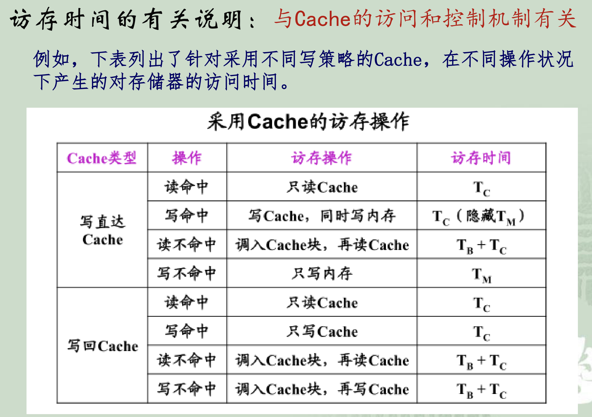
3. Cache
High speed buffer (Cache): When the program is executed , No need to access instructions and data from slow main memory , It is Direct access to this high-speed, small capacity memory , So as to improve CPU Program execution speed .
3.1 Address mapping
- It's all connected
- Direct mapping
- Group Necklace mapping

Its address translation table , Use associative memory . stay TLB(Transition lookaside buffer) in , For each storage unit :
- Effective bit (1 position ):=1 It works .
- It is amended as follows (1 position ): Used when the block data is modified in use .
- For the convenience of replacement , You can use counters ( I guess the dispatcher )
3.2 Replacement algorithm
It's a clear OS Medium Memory Management Dispatch Page Your algorithm .
- RAND: Random
- FIFO: fifo
- LRU
- LFU
- OTP

3.3 Cache Performance analysis
Hit Rate( shooting ): H = N c N c + N m H=\frac{N_c}{N_c+N_m} H=Nc+NmNc
N C N_C NC:Cache Total number of accesses completed .
N m N_m Nm: The total number of times the main memory has been accessed .

Concept , I'm not sure about the HKCEE ?

4. Compare Cache- Main memory & Main memory - Auxiliary deposit


( 6、 ... and ) Processor design
1. CPU Basic composition
- controller : Control unit
- Arithmetic unit : Data processing
- General register group
- (Cache Cache 、 Internal bus, etc )
Arithmetic unit and controller are in Feng · There are two separate components in the Neumann system , But in the modern computer, it has been merged .

This should be the same as the one above 8088 Let's take a look at the register diagram of . There are both internal registers and general registers in the controller , There is no segment register DS、CS、SS、ES.
CPU There is only one bus inside , Is a single bus structure , So for an addition instruction ADD R0,R1 Come on , Use to single bus 、 Two latches and three clock cycles . These three clock cycles use the bus three times .
2. Instruction system design
2.1 Instruction classification

The details of this section are as follows Command system Let's look at this chapter , The key is : For the purpose of an instruction 、 Deposit 、 And take up address space ( Is it a one address instruction or a two address instruction ).
Basic process :

Put a question :

3. Timing control mode
Synchronous control : Command execution or Each control signal in the instruction is uniformly controlled by a predetermined unified timing signal .
Asynchronous control : When the controller sends a certain control operation signal , Wait for the execution part to complete the operation and send it back “ answer ” The signal , Then start a new operation .
( There is no unified clock signal to synchronize the signals , The instruction cycle of each instruction can consist of a number of different machine cycles )
Joint control : Asynchronous Federation + Synchronous control .
( Most of the micromanipulation sequences are scheduled in a fixed machine cycle , For some operations that are difficult to determine the time, the “ The reply ” The way )

4. Command execution
The fetch instruction executes
Be able to write its process , as follows :

5. Micromanipulation
- Micromanipulation : The control signal controls the most basic operation to be performed ( Atomic manipulation ).
- Micro command : Control signal for micro operation , Generated by the controller .
This is also to be able to write , The chestnuts are as follows :

5.1 Microinstruction control domain code
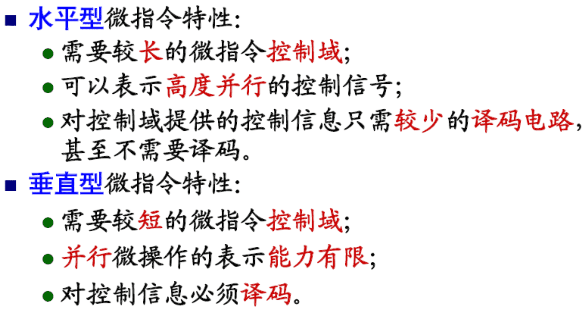
- Horizontal microinstructions : Multiple control signals are effective at the same time , A single microinstruction defines and executes multiple parallel microinstructions .
- Vertical microinstructions :** Different codes of micro operation codes are used to represent different micro operation functions ,** The parallel ability of microinstructions is not emphasized , Usually you can only achieve 1-2 A micro command .
5.1.1 Field decoding method
Divide the control domain into several fields , Vertical coding in the field , Horizontal coding between fields . Mutually exclusive signals are placed in the same field 、 Compatible signals are placed in different fields .
- Compatible signals : Control signals that can be effective at the same time .
- Mutex signals : No more effective control signals at the same time .
5.1.2 For horizontal type & Comparison of vertical type
边栏推荐
- 2D 照片变身 3D 模型,来看英伟达的 AI 新“魔法”!
- Google Earth Engine(GEE)—如何新增一个图例在Map面板
- 如何开发短信通知和语音功能医院信息系统(HIS系统)
- How to export only the titles in word documents? (i.e. delete all the text contents and keep only the title) stop B
- How to write controller layer code gracefully?
- Visual presentation of pictures effectively enhances the attraction of large screen
- 11+文章-机器学习打造ProTICS框架-深度揭示了不同分子亚型中肿瘤浸润免疫细胞对预后的影响
- 为什么虚拟机ping的通主机,主机ping不通虚拟机
- Analysis and understanding of Jieba stutter word segmentation principle HMM application in Chinese word segmentation and partial code reading
- 我在深圳,到哪里开户比较好?现在网上开户安全么?
猜你喜欢

TP-LINK 1208路由器教程(2)
![[graduation season · attacking technology Er] three turns around the tree, what branch can we rely on?](/img/0a/0ebfa1e5c1bea6033b538528242252.png)
[graduation season · attacking technology Er] three turns around the tree, what branch can we rely on?

Qt: judge whether the string is in numeric format

《opencv学习笔记》-- 离散傅里叶变换

Linker --- linker

ArrayList#subList这四个坑,一不小心就中招

How stupid of me to hire a bunch of programmers who can only "Google"!

Understanding of homogeneous coordinates

Turn 2D photos into 3D models to see NVIDIA's new AI "magic"!

计组_cpu的结构和工作流程
随机推荐
Reliable remote code execution (1)
[live review] battle code pioneer phase 7: how third-party application developers contribute to open source
集群控制管理
电商红包雨是如何实现的?拿去面试用(典型高并发)
如何只导出word文档中的标题?(即将正文内容都删除,只保留标题)B站牛逼
【老卫搞机】090期:键盘?主机?全功能键盘主机!
怎么可以打新债 开户是安全的吗
New progress in the construction of meituan's Flink based real-time data warehouse platform
保险APP适老化服务评测分析2022第06期
《opencv学习笔记》-- 感兴趣区域(ROI)、图像混合
≥ 2012r2 configure IIS FTP
Give you a server. Can you deploy your code online?
PHP短信通知+语音播报自动双呼
[digital ic/fpga] booth multiplier
2022年有什么低门槛的理财产品?钱不多
2021-06-03: Boolean operation. Given a Boolean expression and an expected cloth
ahk实现闹钟
《opencv学习笔记》-- 图像的载入和保存
Any and typevar make the automatic completion of IDE better
Programmers spend most of their time not writing code, but...