当前位置:网站首页>FPGA based analog I ² C protocol system design (Part I)
FPGA based analog I ² C protocol system design (Part I)
2022-06-24 15:11:00 【FPGA technology Jianghu】
be based on FPGA The simulation I²C Protocol system design ( On )
Today, I bring you FPGA Of simulation I²C Protocol design , Because of the long space , It is divided into three parts . Today I bring the first one , Part 1 , I²C Bus analysis and simulation I²C Basic framework of interface program . Don't talk much , Loading .
There are also related articles before , Great Xia, you can search by yourself , Source series : be based on FPGA Of IIC Design ( Source attached works ).
Reading guide
I²C(Inter-Integrated Circuit), It's actually I²C Bus abbreviation , Chinese is integrated circuit bus , It's a serial communication bus , Using multi master slave architecture , By Philips in 1980 In order to make motherboard 、 Embedded systems or mobile phones are developed to connect low-speed peripheral devices .I²C The correct reading of is “I square C”("I-squared-C"), and “I Two C”("I-two-C") Is another wrong but widely used way of reading . since 2006 year 10 month 1 The date of , Use I²C The agreement no longer requires the payment of patent fees , But manufacturers still have to pay for I²C Slave device address .
I²C Simply speaking , Is a serial communication protocol ,I²C The communication protocol and communication interface are widely used in many projects , Such as serial in the field of data acquisition AD, Camera configuration in the field of image processing , In the field of industrial control X X-ray tube configuration, etc . besides , because I²C The agreement occupies IO There are very few resources , Easy to connect , Therefore, it is often used in engineering I²C The interface is used as the communication protocol between different chips .I²C A serial bus usually has two signal wires , One is a two-way data line SDA, The other is the clock line SCL. All received I²C Serial data on the bus device SDA All connected to the bus SDA On , Clock line of each device SCL Connected to the bus SCL On .
In modern electronic systems , There are numerous IC Need to communicate with each other and with the outside world . In order to simplify the circuit design ,Philips The company has developed an internal IC Simple bidirectional two-wire serial bus for control I²C(Intel-Integrated Circuit bus).1998 When launched in I²C bus protocol 2.0 version ,I²C The agreement has actually become an international standard .
It's going on FPGA When the design , It is often necessary to provide with the periphery I²C Interface chip communication . For example, low power consumption CMOS Real time clock / Calendar chip PCF8563、LCD Driver chip PCF8562、 Parallel port expansion chip PCF8574、 keyboard /LED Driver ZLG7290 And so on I²C Interface . So in FPGA Middle simulation I²C The interface has become FPGA Develop the necessary steps .
This article will explain in detail in FPGA The chip uses VHDL/Verilog HDL simulation I²C agreement , And compiling TestBench Methods of simulating and testing programs .
The first content abstract : Introduction I²C Bus analysis , Include I²C Bus Overview 、I²C The basic concept of agreement 、I²C Timing requirements of the protocol , Simulations are also introduced I²C Basic framework of interface program and other related contents .
One 、I²C Bus Overview
Let's start with I²C The data format and timing in the protocol are introduced , For places not covered here, please refer to 《THE I²C-BUS SPECIFICATION VERSION 2.1 JANUARY 2000》.
1.1 I²C Bus Overview
I²C As a serial bus standard, the protocol has no data throughput capability of parallel bus , But its following characteristics make it widely used :
- Just two buses — Serial data line SDA And serial clock line SCL;
- Each device connected to the bus can pass through a unique address and a simple host that always exists / Set the address from the node relationship software , The master node can send or receive data ;
- It is a true multi master bus , When two or more master nodes initiate data transmission at the same time , Data corruption can be prevented through conflict detection and arbitration ;
- Serial 8 Bit rate can be achieved in standard mode 100kbit/s, It can be reached in fast mode 400kbit/s, It can be reached in high speed mode 3.4Mbit/s;
- The on-chip filter can filter out the hairy spikes on the bus data line , Ensure data integrity ;
- Connected to the same bus IC The quantity is only affected by the maximum capacitance of the bus (400pF) Limit .
A bus is more than just an interconnect , It also contains all the formats and processes of system communication .I²C The characteristics of bus structure ensure the simplicity of its application , In addition, its complete protocol avoids all confusion 、 The possibility of data loss and obstruction of information .
1.2 I²C The basic concept of agreement
I²C The bus supports any IC Production process (NMOS、CMOS And bipolar ). Serial data line SDA And serial clock line SCL Transfer information between devices connected to the bus . Each device has a unique address as an identification mark ( Whether it's a microcontroller 、LCD Drive memory or keyboard interface ), And both can send and receive data . Obviously LCD The drive only needs to receive data , The memory needs to receive and send data . chart 1 Shown is an example of a high-performance integrated TV .
chart 1 High performance integrated TV
From the picture 1 You can see , application I²C The bus is very convenient . In popular words I²C The hardware design of the bus is to connect SDA and SCL Two lines , rely on I²C The agreement completes the software work . stay I²C The following concepts shall be understood in the agreement .
1) Lord / From the node
The master node is responsible for initializing the data transmission of the bus , And generate a clock signal that allows transmission . At this time, any addressed device is considered as a slave node . When there are multiple master nodes transmitting data on the bus , Each master node generates its own clock signal . All peripheral devices attached to the bus 、 Peripheral interfaces are nodes on the bus .
2) Addressing mode of nodes on the bus
There is only one master on the bus at any time ( Master node ) Realize the control operation of the bus , Addressing other nodes on the bus , Timesharing implementation point - Point data transmission . Therefore, each node on the bus has a fixed node address .
I²C The address of the master node on the bus is given by the software , This address is stored in I²C In the address register of the bus .I²C All peripheral devices on the bus have standard device addresses . The device address consists of 7 Digit composition , It and 1 Bit direction bits constitute I²C Addressing bytes of bus devices SLA(Slave address).
The device address is I²C Address coding inherent in bus peripheral interface devices , The device is given at the factory . The data direction bit specifies the data transmission direction of the master node to the slave node on the bus .
1.3 I²C Timing requirements of the protocol
1) Data transfer timing on the bus
I²C The data transmission sequence on the bus is shown in the figure 2 Shown , The specific steps are as follows .
chart 2 I²C Bus data transfer timing
- First, the master node device sends a start signal .
- Next, the master node device sends the slave node address and the read / write mode , altogether 8 position . Where the slave node address 7 position , How to read and write 1 position .
- The slave device corresponding to the transmission address responds ( namely ACK).
- Start data transfer , There is no limit to the amount of data transmitted . Every byte ( Octet ) Followed by the reply bit of the receiving data party . For example, the master node device reads the slave node data , Send data from node , Master node response ; The master node device writes data to the slave node , The master node sends data , Answer from node .
- End of data transfer , The master node device sends a termination signal to end the whole process .
use I²C There is no limit on the number of bytes transferred after the bus , It only requires the other party to respond to a reply bit after each byte is transmitted . The highest bit of data is sent first (MSB,Most Significant Bit). There is a start signal at the beginning of each transmission , There is a stop signal at the end . After the bus transfers a byte , Through the clock line (SCL) The control of causes the transmission to be suspended . For example, when a peripheral device receives N A period of processing time is required after a byte of data in order to continue to receive subsequent byte data , At this time, after answering the signal, you can make SCL Change to low level control bus pause . If the master node requires bus pause, the clock line can also be kept low to control bus pause .
2) Timing signals on the bus
I²C The bus is a synchronous transmission bus , The bus signal is fully synchronized with the clock .I²C The signals related to data transmission on the bus have start signals S、 Stop signal P、 Answer signal A And bit transfer signal . These signals will be introduced one by one .
(1) Start signal
Start signal (Start Condition) Pictured 3 Shown . At that time, the clock line SCL For high voltage , cable SDA The change from high level to low level will form the starting signal , start-up I²C Bus .
(2) Stop signal
Stop signal (Stop Condition) Pictured 3 Shown . At that time, the clock line SCL For high voltage , cable SDA Changing from low level to high level will form a termination signal , stop it I²C Bus .
(3) Answer signal
Pictured 3 By ACK The first 9 Clock pulses correspond to reply bits , The low level on the corresponding data line is the response signal , High level is a non response signal .
chart 3 Start signal and end signal
(4) Bit transmit signal
stay I²C After the bus is started or after the reply signal 1~8 One clock pulse corresponds to one byte 8 Bit data transfer . During pulse high level , Data serial transmission ; Prepare for data during low level , Allow data level conversion on the bus .
Two 、 simulation I²C Basic framework of interface program
simulation I²C The basic framework of the interface program is shown in Figure 4 Shown .
chart 4 simulation I²C Basic framework of interface program
1) Program interface
Interface for connecting with the application , The data of the application is divided into I²C By agreement SDA To external devices . Include the following :
- clk_I FPGA External clock signal .
- rst_I Synchronous restart signal .
- arst_I Asynchronous restart signal .
- adr_I Slave node address .
- dat_I input data .
- dat_o Output data .
- we_I Write valid signal .
- stb_I Interface valid signal .
- cyc_I Valid bus cycle input .
- ack_o Reply signal output .
- inta_o Interrupt signal output .
2) Clock setting register
I²C The agreement provides 3 Two speed modes : Normal speed mode 100kbit/s、 Fast mode 400kbit/s、 High speed mode 3.5Mbit/s.SCL The frequency of the output clock signal is consistent with the speed mode . Program internal use 5 times SCL The signal acts as a clock , and FPGA The external clock needs to be divided to get the clock used internally by the program .
for example : Use normal speed 100kbit/s,FPGA The external clock is 50MHz, Then the clock setting register needs to be set to (50MHz/5*100kHz – 1=99).
3) Clock generation module
The clock generation module generates 4 times SCL Frequency clock signal , It provides trigger signals for all synchronous actions in the bit transmission control module .
4) Command register
The command register consists of 8 position , It determines whether various timing signals are generated on the bus 、 Read or not / Writing data , The meanings expressed by you are shown in the table 1 Shown .
surface 1 Command register contents
5) Status register
The status register is used to display the status of the current bus , For example, whether a response signal from the slave node is received 、 Are you busy 、 Whether it is transferring data, etc , The specific contents are shown in the table 2 Shown .
surface 2 Status register contents
6) Data transfer register
The data transfer register is used to store the data waiting to be transferred . When passing slave node address information , front 7 Bit saves the slave node address , The last bit saves the read / write command ; When passing ordinary data ,8 Bit holds a byte of data . The specific contents of the data transmission register are shown in table 3 Shown .
surface 3 Data transfer register contents
7) Data receiving register
The data receiving register is used to save the pass I²C The last byte received by the bus , The specific contents are shown in the table 4 Shown .
surface 4 Contents of data receiving register
8) Byte transfer control module
The byte transmission control module controls in bytes I²C Bus data transmission . This module passes the contents of the data transfer register to according to the contents set in the command register I²C The receiving end of the bus , Or from I²C The bus sending end receives the data and saves it in the data receiving register .
9) Bit transfer control module
The bit transmission control module performs in bits I²C Bus data transmission and generation I²C Agreement order ( As in the beginning 、 stop it 、 Repeat start, etc ). The byte transmission control module controls various actions of the bit transmission control module . For example, read a byte of data , The bit transfer control module needs to perform 8 A read command .
10) Data shift register
The data stored in the data shift register is always related to the current data transmission . For example, when reading , The master node passes through the shift register in turn SDA Get it from I²C Data from the sender , After completion, the data is copied to the data receiving register . When writing , The data in the data transfer register is copied to the data shift register , And then one by one SDA Transfer data to I²C The receiving end of the bus .
This is the end of this article , The next one is based on FPGA The simulation I²C Protocol design ( in ),I²C The concrete realization of the agreement , Including the implementation of bit transmission 、 The realization of byte transmission and the realization of program body .
边栏推荐
- Py's toad: a detailed introduction to toad, its installation and use
- 测试 H5 和小程序的区别,你真的知道吗?
- 从pair到unordered_map,理论+leetcode题目实战
- 【比特熊故事汇】6月MVP英雄故事|技术实践碰撞境界思维
- Brief discussion on the implementation framework of enterprise power Bi CI /cd
- A brief introduction to the lexical analysis of PostgreSQL
- 业务与技术双向结合构建银行数据安全管理体系
- 10_那些格調很高的個性簽名
- postgresql之词法分析简介
- Py之toad:toad的简介、安装、使用方法之详细攻略
猜你喜欢

从pair到unordered_map,理论+leetcode题目实战

同样是初级测试工程师,为啥他薪资高?会这几点面试必定出彩

Keyword of ES mapping; Term query add keyword query; Change mapping keyword type
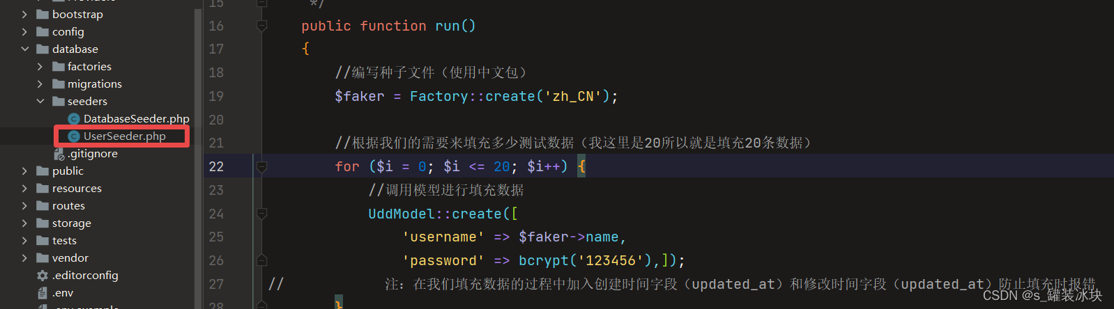
Laravel8 uses faker to call factory to fill data
laravel8使用faker调用工厂填充数据

Overview of SAP marketing cloud functions (IV)

GO语言-goroutine协程的使用

Stm32f1 and stm32cubeide programming examples -ws2812b full color LED driver (based on spi+dma)

laravel 8 实现Auth登录

业务与技术双向结合构建银行数据安全管理体系
随机推荐
【ansible问题处理】远程执行用户环境变量加载问题
3 ring kill 360 security guard process
laravel8使用faker调用工厂填充数据
Detailed explanation of redis data types
3环杀掉360安全卫士进程
June training (day 24) - segment tree
港股上市公司公告 API 数据接口
高薪程序员&面试题精讲系列115之Redis缓存如何实现?怎么发现热key?缓存时可能存在哪些问题?
leetcode 139. Word break word split (medium)
CVPR2022 | 可精簡域適應
The security market has entered a trillion era, and the security B2B online mall system has been accurately connected to deepen the enterprise development path
09_ An efficient memory method
US Senate promotes bipartisan gun safety bill
ESP32系列--ESP32各个系列对比
postgresql 之 ilist
An accident caused by a MySQL misoperation, and the "high availability" cannot withstand it!
左手代码,右手开源,开源路上的一份子
R语言实战应用精讲50篇(二十三)-贝叶斯理论重要概念: 可信度Credibility, 模型Models, 和参数Parameters
15 differences between MES in process and discrete manufacturing enterprises (Part 2)
在CVS中恢复到早期版本