当前位置:网站首页>Chip silicon and streaming technology
Chip silicon and streaming technology
2022-06-22 14:11:00 【wujianming_ one hundred and ten thousand one hundred and sevent】
Chip silicon and flow chip technology
Why are chips so expensive ?
More than one streaming failure , May bring the company down .
The chip industry is no stranger to streaming .
So called streamer , Just like the assembly line, it makes chips through a series of process steps , This link is in the middle stage of chip design and chip mass production , It is the key link of chip manufacturing .
Simply put, it means that the designed scheme , To the chip manufacturer , How many tablets does Mr 、 Dozens of samples , Check whether the designed chip can be used , Then optimize . If the test passes , So we started mass production .
So in order to test whether the IC design is successful , Must be streamed . This is also an important reason why chip design enterprises generally need to invest a lot of costs in the early stage .
A chip from design to mass production , Streaming is a very critical link . When the chip is completely designed, it needs to be etched on the wafer according to the drawing , What kind of process is used , What size wafer , The complexity of the chip will affect the success rate and cost of the chip , And a lot of chips don't make it all at once , In order to obtain ideal results, it is often necessary to tape several times .
But streaming is a very expensive thing , More than one streaming failure , May bring the company down .2019 In, it was reported that Xiaomi's pinecone Electronics' Pengbai S2 Series chips are continuous 5 Secondary streaming failed 、 A painful case of design team reorganization .
Some big chip manufacturers have settled this account ,14nm Process chip , It needs to 300 Around ten thousand dollars ,7nm Process chip , It needs to 3000 Thousands of dollars ,5nm Process chip , One time streaming is to achieve 4725 Thousands of dollars .
so , Streaming is a huge expense for chip design enterprises , Especially for small and medium-sized enterprises in the industry , The actual price of the film is much higher than that of the big manufacturers , Let those who are not rich “ life ” Even worse .
Links to references
https://mp.weixin.qq.com/s/PtubQntH7m7Ca91w9Nl44w
https://mp.weixin.qq.com/s/a0HChvx7U-xmsWRiAlJsgw
Why are streamers so expensive ?
Why is the price of the chip so expensive ?
This brings us to the principle of chip manufacturing .
Chip manufacturing involves putting hundreds of millions of transistors in a very small chip , The manufacturing process has reached the nanometer level , It can only be done by lithography . Lithography is to use light to carve the desired pattern , Lithography requires a mask ( It's also called a mask ,Mask), The mask plate is to engrave the designed circuit diagram on it , Let the light pass , Carve a pattern on a wafer .
Streamer expensive , On the one hand, many processes need to be verified at the beginning , From a circuit diagram to a chip , Check whether each process step is feasible , Check whether the circuit has the required performance and function . The chip flow process lasts at least three months ( Including raw material preparation 、 Photolith 、 doping 、 electroplate 、 Package test ), It usually goes through 1000 Multi process , Longer production cycle , Therefore, it is also the most important and expensive link in chip manufacturing .
If the streaming is successful , Based on this, chips can be manufactured on a large scale ; conversely , You need to find out why , And the corresponding optimization design .
Chip streaming is expensive , Mainly in mask and wafer , These two items are expensive and both are consumables , The mask version is the most expensive , The price of a middle-end process mask is about 50 Around ten thousand dollars , And the price of a wafer is thousands of dollars .
Mask expensive or wafer expensive ?
The mask plate is made of quartz , It is a graphic transfer tool or master in microelectronic manufacturing process , Its function is similar to that of a traditional camera “ negative ”, According to the graphics required by customers , Through the photolithography process , Micro and nano fine patterns are etched on the mask substrate , It is the carrier of graphic design and process technology .
The process of converting this pattern from a mask to a wafer , Imagine the workflow of a money printer . Think of a photolithography machine as a money printer , A wafer is equivalent to a paper for printing money , A mask is a printing plate , The process of printing a banknote master onto paper , Just like the lithography machine prints the chip pattern on the mask onto the wafer .
Lithography requires a mask , The mask plate is to engrave the designed circuit diagram on it , Let the light pass , Carve a pattern on a wafer .
▲ How lithography works
The quality of mask plate will directly affect the quality of lithography , The manufacturing defects and errors on the mask will also be introduced into chip manufacturing along with the lithography process . therefore , Mask plate is one of the decisive factors for the accuracy and quality of downstream products .
The price of the mask mainly depends on the chip “ Process nodes ”, The higher the process node 、 The more expensive the film is . This is because the more advanced the process nodes , The more mask layers you need to use . according to the understanding of , stay 14nm In the process , About need 60 A mask plate ,7nm You may need to 80 There are even hundreds of mask plates .
More layers of mask plate , It's not just because the mask is expensive , And because every extra layer “ Mask plate ”, Just one more time “ Photolith ”, Just apply it again “ Photoresist ”, Just one more time “ Exposure ”, And then one more time “ development ” …, The cost of the whole process is greatly increased .
According to the IBS data , stay 16/14nm In the process , The cost of the mask used is 500 Around ten thousand dollars , To 7nm In the process , The cost of mask rises rapidly to 1500 Thousands of dollars .
▲7nm In the process , The mask cost is about 1500 Thousands of dollars ( Picture source :IBS)
The total cost of the mask , Including quartz , The cost of raw materials such as photoresist ,Mask Writer and Inspection The use cost of such machines , In addition, there is the generation of mask related data , Include OPC、MDP And so on 、 Server usage and labor development costs, etc . For a chip , Dozens of layers of mask plates , It takes so many steps , equipment 、 Software 、 Personnel are indispensable , The cost is naturally expensive .
In the streamer ,Mask The cost of is a big part , The reason is that the early stage of production is production 5-25 Tablets are used for product verification , The main cost is Mask cost . Corresponding , During formal production ,Mask The cost of is calculated only once , There are a large number of wafers to share the cost , Naturally, it's cheaper .
To be exact, the average cost of each chip is cheaper , Instead of the total cost of the film is cheaper .
According to insiders , A wafer foundry (Foundry) 40nm The cost of the film is about 60-90 Thousands of dollars .Mask Take the lead , about 60-90 Thousands of dollars ; The cost per wafer is at 3000-4000 About $ .
therefore , If you produce 10 Wafer wafer , The cost per wafer is (90 ten thousand + 400010)/10=9.4 Thousands of dollars ; But if production 10000 Wafer wafer , So the cost per wafer is (90 ten thousand +400010000)/10000=4090 dollar .
so , After entering mass production , Produce tens of thousands of wafers , Each wafer may 3000-4000 About $ ,Mask After the cost is spread to each wafer, it will be very small , At this time, the cost of wafer is the main source of cost . therefore , If it is only a small amount of film stage , that Mask Cost is the main . On the contrary, if mass production is a lot , Then it is the dominant cost of the wafer .
in addition , The machines in semiconductor manufacturing plants cost millions of dollars , Hundreds of millions of dollars . according to the understanding of ,28nm Of Mask The machine exceeds 5000 Ten thousand dollars a set , These instruments , The machine needs to be depreciated for seven years . in other words , It will lose about one year 14% The value of the machine .
The depreciation life of equipment in the foundry industry is usually 5-7 year . As report goes , smic 2019 The annual depreciation expense exceeds 14 Billion , This is mainly because the investment in advanced manufacturing process requires the purchase of some machinery and equipment with high unit price , The depreciation cost increases year by year . TSMC 2021 The annual depreciation cost has reached nearly NT $100 billion , The highest in history .
In terms of process R & D cycle , The cost and depreciation of machines are already high , But it is also a challenging task to adjust the yield and reliability of the process to the requirements of mass production .( It is reported that a factory engaged in 28nm, machine 2011/2012 It will be all in place in , But 5、6 Years later, the yield has not been adjusted to the strict mass production standard , You can see how difficult it is . At the same time, the equipment depreciation cost for many years has been lost in vain .)
Then there is the cost of manpower , Maintenance costs, consumables, etc , These are all Mask The reason for the high cost .
According to the etnews reports , As the current supply and demand situation worsens , The price of mask is still rising , The delivery time has also been repeatedly delayed , Even if you pay extra , It is also difficult to buy in time . Usually 4-7 The delivery date of days has recently increased to 14 God , The delivery time of some enterprises has been extended to the original 7 times .
Besides , To keep up with Moore's law ,Foundry The investment in R & D of equipment and technology required for upgrading is increasing , because Foundry Huge investment in advanced production lines , It will inevitably transfer the cost to the customer's investment expenses . This has also led to the rising cost of making chips .
How to reduce the production cost ?
Under the influence of the above factors , The cost of chip streaming has become a difficult problem for design enterprises . that , Facing the problem of high film price , Is there any way to reduce costs ?
Wanglong, senior director of Moore elite, said to the author ,MPW(Multi Project Wafer) It is a kind of streaming method that can help design enterprises reduce costs .
MPW It means that a wafer is shared by multiple projects , The same manufacturing process can undertake multiple tasks IC Design manufacturing tasks , Multiple IC designs using the same process are streamed on the same wafer , After manufacturing , Dozens of chip samples can be obtained for each design , This amount is important for the experiments in the prototype design stage 、 Testing is enough .
Generally speaking, it means that several companies or institutions buy a set of mask plates together , Then there will be several chips on the same wafer , After wafer cutting , And then put their chips “ Take home ”. The manufacturing cost shall be borne by all participants MPW According to the chip area , It greatly reduces the risk of product development .
According to Wang Long ,MPW There is a certain process , It is usually organized by a wafer foundry or a third-party service organization , All kinds of craft in a certain year MPW The time point is preset , Usually, the more advanced the technology , Arrange the MPW The higher the frequency is. . The wafer foundry will divide the wafer into several areas and quote in advance , Companies book one or more areas according to their own conditions .
This is for participants , There is certain progress pressure in design and development . But by contrast ,MPW The benefits are clear , Using multi project wafers can reduce the production cost of chips , Provide practice opportunities for designers , And promote the achievement transformation of chip design , Yes IC Training of design talents , The development of small and medium-sized design companies , And the development of new products have a considerable role in promoting .
By contrast , share Mask The good thing is to save money , But we may have to wait for the time node of the OEM , It takes more time . Those enterprises that are not short of money or in a hurry can of course make use of one set by themselves Mask(Full- Mask, Full mask ), All masks in the manufacturing process serve their own design , It is usually used in the mass production stage after design finalization . When the machine rings , Gold two thousand .
however , In the current situation of serious capacity shortage , The OEM faces the product needs of different customers 、 competitive edge 、 The attitude of market prospect and plan is totally different , The OEM will comprehensively consider the quantity of orders placed by customers , The stability of subsequent orders and the market prospect the product faces .
actually , For most small and medium-sized enterprises , Except for the price , In the flow or mass production process, the production capacity is also faced 、 Many challenges including delivery time :
1. Yes Foundry The system doesn't understand , Lack of experience and experience in process selection Foundry Experience in dealing with ;
2. Main stream Foundry The entry threshold is high , It is difficult for emerging players to apply for the expected process or support , High communication cost ;
3. Lack of systematic supply chain management ability , Especially in the ramp up stage of mass production capacity , Yes 、 Delivery date 、 The quality is too optimistic ;
4. In case of capacity shortage , Lack of stock mechanism , Panic orders or orders with orders lead to production capacity not keeping up with market demand . Besides , Change of delivery date 、 Fluctuations in production capacity will greatly increase the communication costs between start-ups and foundries , Reduce efficiency .
Regarding this , Small and medium-sized chip design enterprises can seek resources 、 Have the strength 、 Cooperation with experienced third-party operation service agencies , Together to solve the supply chain problems encountered . No matter from technology 、 Business or production capacity , Choosing a reliable third-party organization can help the design company solve the current supply chain difficulties , Provide the optimal solution .
To make a long story short , Companies in these demand tracks are likely to benefit from the business of streaming service providers .
Conclusion
A chip development project , Need to experience from product definition 、 Design 、 The long process from validation simulation to final streamer , And as a “ The final exam ” Streamer of , Any small mistake in the long process before may lead to the failure of streaming , However, once the film production fails, it often means that the enterprise will face losses of tens of millions of dollars and missed market opportunities for at least half a year .
For many enterprises , The failure of streaming film is unbearable pain .
Regarding this , Chip design enterprise 、 Manufacturers and relevant industry service platforms and institutions shall cooperate closely , Complementary advantages , Work together to solve the problems that puzzle developers “ The problem of streaming ”.
Throw again 68 One hundred million yuan ! The war on domestic large silicon wafers has been upgraded ,7 Big players charge , Who can take the lead to the top ?
The global silicon wafer production is expanding wildly , The Chinese mainland 12 The monthly production capacity of inch silicon wafer will exceed 265 ten thousand !
Core thing 6 month 2 Reported Wednesday , On Thursday, , Shanghai Silicon Industry Group Co., Ltd ( hereinafter referred to as “ Shanghai silicon group ”) Its subsidiary Shanghai Xinsheng will contribute 15.5 One hundred million yuan , Co invest with multiple investors such as the second phase of the large fund 67.9 One hundred million yuan , Build a port in Shanghai 30 For ten thousand integrated circuits 300mm(12 Inch ) High end silicon wafer expansion project . This is the successor to Germany Shichuang (Siltronic)、 Japan wins high (SUMCO)、 Taiwan, China universal wafer and Korea SK siltron Since last year, the four international giants 10 The month after month has been exposed 、 Announce investment and expansion of production 300mm Behind the silicon wafer , The latest production expansion of silicon wafer players in Chinese Mainland . Silicon chip is the main material for chip manufacturing , It is the material with the highest proportion in the cost of chip materials .2021 In the global core shortage tide , Shinyue chemical, which accounts for more than half of the market in Japan 、 Japan wins high (SUMCO) The two silicon chip leaders first raised their prices , This has driven up the cost of wafer manufacturing in the downstream . by comparison , The market share of silicon wafer manufacturers in Chinese Mainland is small , And mainly 200mm(8 Inch ) And the following sizes of silicon chips , It is difficult to satisfy the local people 300mm(12 Inch ) Demand for wafer manufacturing .2017 year ,“ The godfather of China's semiconductor industry ” Shanghai Xinsheng founded by zhangrujing realized for the first time 300mm Silicon wafer mass production , It breaks the monopoly of international giants on large silicon wafers . Now besides Shanghai silicon group , Liangwei 、 Zhonghuan Co., Ltd 、 Super silicon semiconductor 、 Zhongxin wafer 、 Yisiwei and other mainland silicon chip players have also realized 300mm Mass production of silicon wafer , Youyan silicon is under construction 300mm Silicon wafer production line , These domestic silicon wafer enterprises are becoming new forces to enter the large silicon wafer market . According to incomplete statistics , Current domestic silicon chip players 300mm The total capacity of silicon wafer has exceeded 162 Ten thousand pieces / month , Waiting for Shanghai silicon group 、 After the new production lines of players such as Zhonghuan shares and yisiwei are put into production , domestic 300mm Silicon chip capacity may exceed 265 Ten thousand pieces / month . This article benefits : The global semiconductor silicon wafer industry is highly concentrated , The process of domestic substitution has accelerated . Recommend high-quality research report 《 In depth report of semiconductor silicon wafer industry 》, You can reply to key words in official account chat bar. 【 Core thing 266】 obtain .
Zhangrujing founded Shanghai xinshengcong 0 To 1 Realize mass production of large silicon wafers
Silicon chip is the cornerstone of the semiconductor industry , Silicon chips for integrated circuits have high requirements for purity and surface cleanliness , To avoid internal defects , Its purity is generally at 11 individual 9 above (99.999999999%), The content of impurities on the surface shall be less than 1 / 10 billion . Under the influence of Moore's law , To reduce chip costs , The size of silicon wafer is getting larger and larger . The larger the diameter of the semiconductor silicon wafer , The more chips can be produced on a single silicon chip , The smaller the edge loss , The lower the cost of a single chip .
▲200mm Silicon wafer and 300mm The difference between silicon wafers ( picture source : Pioneering securities )
Under the same process ,12 The usable area of inch silicon wafer exceeds 8 Inches of silicon 2 times , The availability rate is 8 Inches of silicon 2.5 About times . At present, the world's mainstream silicon wafer specification is... In diameter 200mm(8 Inch ) and 300mm(12 Inch ) Silicon wafers ,7nm And the following advanced process chips are also being promoted 300mm Demand for silicon wafers is growing . according to SEMI( International Semiconductor Industry Association ) data ,2019 year , The global 300mm The proportion of silicon wafer shipping area has reached 67.22%.
▲2019 year -2025 year ,7nm And 5nm And the following advanced processes 300mm Silicon wafer production capacity ( picture source : Japan wins high )
Besides , since 2021 The chip shortage began in , Promoted the global wafer factory construction upsurge ,2020 year -2024 year SEMI It is expected to add 30 More than 300mm fabs , Among them, Chinese Mainland will add 8 home , mainland 300mm The share of chip capacity in the world will increase from 2015 Year of 8% Up to the 2024 Year of 20%, That's all right 300mm The capacity of large silicon wafers has put forward the demand . Contrary to the rising demand , stay 300mm On a silicon chip , The capacity of silicon wafer manufacturers in Chinese Mainland is insufficient 、 Low market share , Of local wafer manufacturing enterprises 300mm Silicon wafers are mainly imported , Rely on Japan 、 South Korea 、 Taiwan, China and other countries and regions . Until 2017 year , Shanghai Xinsheng semiconductor has become the first mass production enterprise in China 300mm Silicon wafer enterprises . Shanghai Xinsheng was founded in 2014 year 6 month , Founded by zhangrujing, founder of SMIC , It's the first one in China 300mm The implementation subject of the large silicon wafer project , Assumed the responsibility of the state 02 In the special project “40-28 For nano integrated circuit manufacturing 300 Mm silicon wafer ” project .
▲ Shanghai Xinsheng “40-28 For nano integrated circuit manufacturing 300 Mm silicon wafer ” The foundation laying ceremony of the project ( picture source )
After leaving SMIC , Zhangrujing founded 、 Invested in Yingrui optoelectronics and other companies LED company . After the non competition period , He was invited to establish Shanghai Xinsheng semiconductor in Shanghai Lingang heavy equipment zone , Controlled by Shanghai silicon industry , With a total investment of about 68 One hundred million yuan , Focus on 300mm Silicon . The establishment of Shanghai Xinsheng , From the beginning, it was for breakthrough 300mm Process and technical bottleneck of large silicon wafer . Shanghai Xinsheng is absorbing international 300mm On the basis of silicon chip technology , Solved domestic problems through R & D and innovation 300mm The situation that silicon wafers depend on imports .2015 year , The construction of Shanghai Xinsheng phase I plant started ,02 Special “40-28nm For integrated circuit manufacturing 300mm Research and development of silicon wafer technology ” The foundation stone laying ceremony was held for the project ;2016 year , The first crystal rod goes offline ;2017 In, Shanghai Xinsheng realized mass production , And the first product is sold .
▲ The first batch of Shanghai Xinsheng 300mm Large silicon wafer single crystal rod
2017 In, Shanghai Xinsheng realized 300mm After silicon wafer mass production , Zhangrujing's term of office expires , Announced to leave Shanghai Xinsheng . For this departure , Zhangrujing said frankly ,300mm Silicon wafers are originally made for the country , by comparison , Yes IDM( Vertical manufacturing mode ) More interested in . Zhangrujing's departure has not slowed down the development of Shanghai Xinsheng ,2018 Its positive film passed the certification in , Monthly production capacity reaches 10 Ten thousand pieces / month ;2019 year , Shanghai Xinsheng 28nm Logic 、3D NAND Storage positive certification passed ;2020 Advanced process logic certification in , Its 02 special “40-28nm For integrated circuit manufacturing 300mm Research and development of silicon wafer technology ” The project has passed the acceptance ;2021 The second year 30 Ten thousand pieces / The construction of the plant started in January .
▲ President of Shanghai silicon industry group 、 Shanghai Xinsheng CEO Qiuciyun
2021 At the China IC Annual Conference , President of Shanghai silicon industry group 、 Shanghai Xinsheng CEO Qiuciyun concluded that , Shanghai Xinsheng makes new moves every year . In this investment 67.9 The 100 million yuan project is expected to 2024 Reach production capacity at the end of the year , After the completion of the project, Shanghai Xinsheng will add 30 Ten thousand pieces / month 300mm Semiconductor silicon wafer capacity , Its integrated circuit uses 300mm The total capacity of semiconductor silicon wafer will reach 60 Ten thousand pieces / month . from 2014 So far this year , Shanghai Xinsheng and the Shanghai silicon group behind it have achieved... In Chinese Mainland 300mm Large silicon wafers from 0 To 1 Breakthrough .
domestic 300mm In the future, the expansion of the large silicon wafer Corps will reach 265 Ten thousand pieces / month
In recent years , The development of silicon wafer industry in Chinese Mainland has accelerated , Besides Shanghai silicon group , And central shares 、 Liangwei 、 Max 、 Zhongjing technology and other listed companies , Youyan silicon and other enterprises are also sprinting on the scientific innovation board . Nowadays, it has been used for integrated circuits 300mm Listed companies with large silicon wafer mass production capacity include Shanghai silicon group 、 Zhonghuan shares and Leon micro , Besides , There is grinding silicon 、 Super silicon semiconductor 、 Domestic silicon chip players such as Zhongxin wafer and yisiwei have also entered 300mm Silicon age . According to Shanghai silicon group 、 The annual reports of Zhonghuan shares and lion micro , Three companies 300mm The capacity of silicon wafer is 30 Ten thousand pieces / month 、17 Ten thousand pieces / The month and 180 Ten thousand pieces / year , The total is about 62 Ten thousand pieces / month ; Zhongxin wafer and yisiwei 300mm The capacity of silicon wafer is 240 Ten thousand pieces / Years and 50 Ten thousand pieces / month , The total is about 70 Ten thousand pieces / month ; According to media reports , Super silicon semiconductor 300mm The capacity of silicon wafer is about 30 Ten thousand pieces / month . at present ,7 The total production capacity of the projects put into operation by the company is about 162 Ten thousand pieces / month .
▲ According to incomplete statistics , By 2021 At the end of the year, Chinese Mainland 300mm Silicon wafer capacity
Zhonghuan Co., Ltd. was established in 1999 year , Headquartered in Tianjin , Formerly known as 1969 Tianjin No. 3 semiconductor device factory founded in , The main business includes integrated circuit silicon wafer and photovoltaic silicon wafer .2017 year , Zhonghuan shares started in Yixing, Jiangsu Province 300mm Large silicon wafer production and manufacturing project for integrated circuits , The total investment reaches 30 Billion dollars . The first phase of the project has been completed in 2020 year 9 Put into production in ,300mm The monthly production capacity of silicon wafer reaches 15 Ten thousand pieces . By 2021 end of the year , Zhonghuan Co., Ltd 300mm Silicon chip capacity reaches 17 Ten thousand pieces / month , Expect to 2023 By the end of the year 300mm 60 Ten thousand pieces / The size of the month . It is worth noting that , Most of the revenue of Zhonghuan shares comes from the new energy photovoltaic industry , Its 5 month 26 On the th, it announced that it would change the raised funds , Use the original for “ For integrated circuits 8-12 Inch semiconductor wafer production line ” and “ Replenish working capital ” The balance of the two items 9.76 Billion yuan invested in “ Annual output of 30GW High purity solar ultra-thin silicon single crystal material smart factory ” In the project . announcement , This change will not affect the progress of subsequent projects .
▲ Description of the raised funds for the change of Zhonghuan shares
Leon micro was founded in 2002 year 3 month , The current headquarters is located in Hangzhou , The founder is academician que duanlin . One of the first scientists in China to study silicon materials , Former vice president of Zhejiang University ,1991 He was elected academician of the Chinese Academy of Sciences .2000 year , He founded Zhejiang jinruihong Technology Co., Ltd. with Professor liliben ,2010 Has undertaken 02 Special “200mm Silicon wafer R & D and industrialization 300mm Research on Key Technologies of silicon wafer ” project . Now jinruihong technology is one of the subsidiaries of Leon micro .
▲ Academician que duanlin, founder of Zhejiang jinruihong
Lion micro's main business includes semiconductor silicon chips 、 Semiconductor power device 、 Compound semiconductor RF chip , Its 300mm The silicon wafer production line is built in Quzhou, Zhejiang Province , The annual production capacity has reached 180 Ten thousand pieces , covers 14nm The above process . Leon micro 300mm Silicon wafers have been shipped on a large scale in image sensor devices and power devices , Currently, it mainly sells 300mm Silicon wafer products include polished wafer, test wafer and epitaxial wafer . Youyan silicon was founded in 2001 year 6 month , The registered capital is about 10 One hundred million yuan , Headquartered in Beijing , Formerly known as Youyan Technology Group Co., Ltd ( Former Beijing Nonferrous Metals Research Institute )401 room , Since the last century 50 In the s, he began to study silicon materials . According to its prospectus ,2006 year , There is research on silicon development 12 Inch silicon wafer process research ,2020 At the end of the year 300mm The large silicon wafer project for integrated circuits started in Dezhou, Shandong Province , The estimated capacity is 360 Ten thousand pieces / year .
▲ Youyan silicon company
Zhongxin wafer was founded in 2017 year , Headquartered in Hangzhou ,2020 After internal integration in , Covering the business of Ningxia Zhongxin wafer semiconductor technology Co., Ltd. and Shanghai Zhongxin wafer semiconductor technology Co., Ltd , From semiconductor monocrystalline silicon rod to 100mm/200mm/300mm Silicon wafer production capacity , Its 300mm Annual capacity of silicon wafer 240 Ten thousand pieces , About us 20 Ten thousand pieces / month . Easyway was founded in 2016 year 3 month , Headquartered in Beijing , The business covers chips 、 Silicon materials and advanced sealing and testing . Its current chairman is wangdongsheng, founder of BOE .2019 year 6 After stepping down as the chairman of BOE in June , Invited to join yisiwei ,2020 year 2 In June, he was appointed chairman of easyway .2017 Fourth quarter of 2007 , Easyway launched in Xi'an 300mm Silicon wafer project , The total investment 110 One hundred million yuan , In two phases . The capacity of its phase I plant is 50 Ten thousand pieces / month , The products are polished wafers and epitaxial wafers , Mainly used in logic chips 、 Flash memory chips 、DRAM Memory chips 、 Image sensor and display driver chip . Supersilicon semiconductor was founded in 2008 year , Headquartered in Songjiang, Shanghai , Chongqing super silicon is its subsidiary , Focus on 200mm Silicon . Shanghai Super silicon focuses on 300mm Polishing sheet and thin epitaxial sheet, etc , Its Shanghai plant has been in 2020 Annual operation . According to media reports , Shanghai Super silicon 300mm Capacity up to 30 Ten thousand pieces / month . Japan Shenggao estimates ,2024 year , The global 300mm Demand for silicon wafers will approach 900 Ten thousand pieces / month ; To 2026 year , The global monthly demand will exceed ten million pieces . by comparison , Domestic players 300mm The silicon chip production capacity may still lag behind the international silicon chip giants .
▲2019 year -2026 year , The global 300mm Silicon wafer demand forecast ( picture source : Japan wins high )
Business transformation 、 Mergers and acquisitions 、 State owned assets participate in building domestic large silicon chip players
From the growth process of domestic players , The listed Shanghai silicon group 、 Zhonghuan Co., Ltd 、 Leon micro and Youyan silicon, which is sprinting the scientific innovation board, respectively present different development paths and directions . Shanghai silicon group is realizing 300mm After silicon wafer mass production , Acquired Finland, the seventh largest silicon wafer manufacturer in the world Okmetic, And by subscribing to France Soitec The private placement of shares became the SOI One of the largest shareholders of the silicon chip leader . Zhonghuan Co., Ltd. and Leon micro span from other businesses to the field of silicon chips for integrated circuits . The business of Zhonghuan Co., Ltd. mainly includes photovoltaic silicon wafers and silicon wafers for integrated circuits ,2021 In, its revenue in the new energy photovoltaic field accounted for more than 93.54%, The income of semiconductor industry only accounts for 5.17%; Leon micro business includes semiconductor silicon chips 、 Semiconductor power devices and compound semiconductor RF chips , Its 2021 The sales revenue of silicon wafer accounted for 57.4%.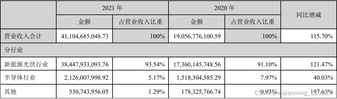
▲ Zhonghuan Co., Ltd 2021 Proportion of business income in ( picture source : Zhonghuan Co., Ltd 2021 Annual report )
Youyan silicon is from Youyan Technology Group Co., Ltd ( Former Beijing Nonferrous Metals Research Institute ) Of 401 room , Since the last century 50 Silicon material research began in the s , It has accumulated technology for more than half a century . Now its controlling shareholder is Japan Co., Ltd RS Technologies, The company is currently the world's largest semiconductor wafer recycling manufacturing enterprise ( Individual holding , SASAC's indirect equity participation ). The combination of the two has created today's silicon .
▲ Youyan silicon's shareholding structure
From the development of domestic large silicon chip players nowadays , Business transformation of silicon material enterprises 、 Enterprise merger and acquisition and state-owned capital investment , It plays an important role in promoting the development of domestic large silicon wafers . But if you trace the source , It is still inseparable from the independent process 、 Technological breakthroughs , This will still be the foundation of domestic silicon chip industry in the future . In Shanghai silicon group 、 Zhonghuan Co., Ltd 、 Liangwei 、 Domestic silicon wafer players such as Youyan silicon have increased production 、 While building the plant , Japan wins high 、 China Taiwan global wafer 、 Germany and Korea SK siltron And other international giants are also increasing investment , Set off a wave of factory construction . Shenggao plans to invest 20.5 Billion dollars , A new plant will be built next to its existing plant in Saga Prefecture, Japan , Manufacturing for advanced process logic chips 300mm Silicon , It is expected that 2023 It will be put into operation by stages in the second half of the year . Universal wafer failed to acquire Shichuang , But in Asia 、 Europe and the United States and other places invest in construction 300mm、200mm、SOI Silicon 、SiC Silicon chip, etc , The total investment amount exceeds NT $100 billion , The new production line will start from 2023 It has been put into operation since .
▲ Universal wafer failed to acquire Germany Shichuang 、 The announcement that the company will invest in building a factory instead ( picture source : Universal wafer )
Shichuang also plans to invest 7.9 Billion dollars , Build a new plant in Singapore , production 300mm Silicon , Is due to 2024 Put into production at the beginning of the year .SK siltron Plan to invest 8.6 Billion dollars , Expand its plant in Kuiwei, South Korea , enlarge 300mm Silicon wafer production capacity , Is due to 2024 Large scale production in .
Domestic large silicon wafers are expanding production or will break the international leading monopoly
Silicon chip is one of the most important chip materials , It plays an important role in the supply chain .2020 The global core shortage started in the second half of the year , Total occupied 50% Japan Shenggao and shinyue chemical, with the above market share, took the lead in raising prices , Occupy the initiative of bargaining . since 2017 Since then , Domestic silicon wafer enterprises led by Shanghai silicon group are rapidly expanding production , Enter 300mm Large silicon wafer market , Improve the position and market share of the domestic silicon chip industry , Or it will break the monopoly of international leaders , Take the initiative in the supply chain .
Links to references
https://mp.weixin.qq.com/s/PtubQntH7m7Ca91w9Nl44w
https://mp.weixin.qq.com/s/a0HChvx7U-xmsWRiAlJsgw
边栏推荐
猜你喜欢

Oceanbase database helps the ideal automobile intelligent production line to realize automatic recovery within 30 seconds

Traffic replication in istio Service Grid

BSN发展联盟理事长单志广:DDC可为中国元宇宙产业发展提供底层支撑

HMS Core新闻行业解决方案:让技术加上人文的温度

Simple integration of client go gin IX create

transformers VIT图像模型向量获取

Tasks and responsibilities of the test team and basic concepts of testing

JasperReport报表生成工具的基本使用和常见问题

"Dare not doubt the code, but have to doubt the code" a network request timeout analysis

VR panoramic shooting breaks the deadlock of traditional propaganda that wild geese pass without leaving traces
随机推荐
After several years of writing at CSDN, I published "the first book". Thank you!
polardbx是pg还是mysql?
别再用 System.currentTimeMillis() 统计耗时了,太 Low,StopWatch 好用到爆!
How do I open an account on my mobile phone? Is it safe to open an account online?
七牛云上传图片
机器人方向的刚性需求→个人思考←
SQL functions -- converting a one to many relationship to a one to one relationship
Oracle stored procedure 2
leetcode-数学题
芯片硅片与流片技术
Word skills summary
安装和使用protobuf-c
融云:让银行轻松上“云”
"Dare not doubt the code, but have to doubt the code" a network request timeout analysis
天润云上市在即:VC大佬田溯宁大幅减持,预计将套现2.6亿港元
History of hash index design
Offline physical stores combined with VR panorama make virtual shopping more realistic
Leetcode math problems
Are you familiar with redis cache of highly paid programmers & interview questions series 114? How are redis keys designed? Are you familiar with the memory obsolescence mechanism?
Record the solution of failing to log in after the alicloud ECS instance is restarted (hands-on practice)