当前位置:网站首页>Design of digital oscilloscope based on arm and FPGA -- QMJ
Design of digital oscilloscope based on arm and FPGA -- QMJ
2022-07-24 12:06:00 【Rehabilitation2018】
List of articles
Preface
This design is a 4 Channel portable digital oscilloscope , use DE1-SOC Design with dual core development board . The digital to analog converter of oscilloscope adopts LCT2308 Chip implementation . The design of the whole system consists of two parts , One is to complete FPGA Design of hardware circuit ; The two is the use of ARM Design the software function of the system .
This portable digital oscilloscope has small volume 、 Advantages of light weight and low power consumption . The tools used include :Quertus II 18.0,Modelism, Logic analyzer , The embedded linux -SD System startup card .
Currently implemented functions , The waveform signal can be adjusted to translate up and down in the display , Time axis zoom and vertical axis zoom .
One 、 Portable digital oscilloscope design
1.1 Design principles and ideas
The oscilloscope design is shown in the figure 1-1 Shown ,DE1-SOC The development board passes the onboard LCT2308 The chip collects analog signals . Use ARM Through lightweight HPS-to-FPGA Bridge connected IP nucleus PIO, control FPGA modular , this IP nucleus PIO Is defined as CFG port .CFG The port will transmit continuously 32bit data , among 8bit Used to identify FPGA modular , rest 24bit Belong to FPGA Control parameters of the module .
adc.v Module through SPI Bus and LCT2308 Chip connection , And from LCT2308 The chip is set in the sampling channel to obtain waveform data .
Then send these waveform data to time_scaler.v modular , The module uses N Waveform data discarded N-1 To achieve the required effective sampling rate .
The waveform data is transmitted to the trigger module , These waveform data are also passed to the trigger module , The trigger module will wait for the trigger signals from the outside and from the trigger module . When two trigger signals occur , The trigger module starts to store the next 640 Data points , And write the waveform data to the on-chip memory SRAM.
vga.v Read the waveform data in the on-chip memory , Convert waveform data into pixel data and send it to VGA.
1.2 System technical indicators
Waveform voltage :0V~4.096V
Measurement frequency range :0~500KHz
Storage depth :640
Sampling channels :4 passageway
display mode :640*[email protected]
VGA clock frequency :25MHz
FPGA clock frequency :50MHz
Two 、 The functions of each module of the oscilloscope
2.1 LCT2308 Introduce
DE1-SOC Development board on board LCT2308(ADC) Structure is shown in figure 2-1 Shown , Is a 12bit High precision successive approximation analog-to-digital conversion chip , Have 8 Analog input channels , With as much as 500 kSPS Mining Sample rate and a compatible serial peripheral interface (SPI) .

SPI The bus includes 4 Logical lines , The definition is as follows :
CONVST: Piece of optional signal , Sent by the host , To control the communication with the slave , Low level is an effective signal ;
SCK: Serial clock signal , Generated by the master and sent to the slave ;
SDI: Host output , Slave input ( The data comes from the host ), choice LCT2308 Sampling channel of ;
SDO: Host input , Slave output ( The data comes from the slave ), Transmit sampling data .
notes : The side on which the clock is generated is called the host , The other side is called the slave .
2.2 adc.v Module introduction
LCT2308 Sample a point on the waveform , Quantized and coded as 12bit data , adopt SPI Bus transmission to adc.v modular .adc.v The module will pass through figure 2-3 Of FSM The process continues to receive 4 Waveform data of channels , And integrate into 48bit.FSM be in WRITE The status will set a valid flag bit data_val, Feed back the data transmission signal to time_scaler.v modular .

stay FPGA During the operation of the development board , It can be detected by logic analyzer FPGA Changes in data in the module . chart 2-4 in test3 Port means adc.v Change of module state machine ;test1 Ports represent sampling channels 1 The data of ;test2 Ports represent sampling channels 2 The data of ;data_out The data obtained by the port from the sampling channel is integrated 48bit.
2.3 time_scaler.v Module introduction
The module starts from adc.v Every... Received in the module N+1 Deleted from samples N Samples , Realize the horizontal scaling of the display waveform ,N Value can be passed through CFG Configuration register for configuration . The concrete implementation is accomplished by creating a counter , The counter is in adc.v The module increments each time it passes samples , And in achieving N Value is reset to 0. The sample is only when the counter is 0 When passing to the next stage .
chart 2-5 in , Use test1 Port detection counter change ;out_msg The port receives data from adc.v Modular 48bit Waveform data . When the counter is 0 when , Transfer the corresponding waveform data to the next trigger.v modular .
2.4 trigger.v Module introduction
stay ARMED State, , buffer left_buffer Need to save 320 Data points . When the buffer is saved to 320 Data points ,FSM Will enter READY state , Wait for two trigger signals , While waiting for the trigger condition , buffer left_buffer Continuously update data points . When the trigger condition is met , have other 320 Data points in TRIGGERED The status is sent to the buffer right_buffer.
When the buffer right_buffer preservation 320 Data points , Will be in FLUSH_LEFT State and FLUSH_RIGHT Status buffer left_buffer and right_buffer The data points of are written into the on-chip memory SRAM.FSM Get into SEND_REFREESH state , Will send to vga.v The module indicates new data .

trigger.v Modules in READY Status waiting to receive two trigger conditions , They are from triggerer.v Module and external signals . The external signal is triggered by the key ,triggerer.v The module can trigger edges and pulses , The five supported modes are rising edge 、 Falling edge 、 Pulse greater than 、 The pulse is less than and equal to .

chart 2-7 in test1 Detect the state machine of the module ;test2 Detect the simultaneous presence of two trigger signals ;test3 and test4 Detect that the state machine is FLUSH_LEFT and FLUSH_RIGHT State, , On chip memory storage channel 1 And channel 2 Of 640 Waveform data points .
2.5 vga.v Module introduction
vga.v The module receives from trigger.v Modular “go_val” The signal of , Start extracting data from on-chip memory .FSM Of FETCH Status will receive 48bit The data is separated into 4 individual 12bit, And zoom in proportionally .PRCOESS and DRAM The state converts the waveform data into rgb, How to achieve , Prepare two zero setting counters , Counter A from 0 Count to 479, Counter B Add 1, Until the counter B be equal to 639.
This process counter B Every change , To counter A Send a by 12bit convert to 11bit Waveform data , Compare the waveform data with the counter A Numerical comparison , Equal condition rgb For channel waveform rgb, otherwise rgb by 0, It's black .

chart 2-9 in test1 Express vga.v The state machine of the module changes ;test2 Detection counter A;test3 Detection counter B;test4 It means to get rgb data .
3、 ... and 、VGA Two methods of pixel data transmission
For this design ,vga.v Modular rgb The process of transferring data to the display , Separate application PIO Patterns and DMA Pattern to implement .
DMA In mode ,CPU Not fully involved in data transmission , Just give orders .DMA There are controllers and channels under the mode ,CPU Just ask DMA The controller commands , Give Way DMA Controller to handle the transmission of data , After data transmission, the information will be fed back to CPU, That's a lot of relief CPU Resource share .
PIO Mode through CPU To control the data transmission between hard disk and memory , It's a kind of passing CPU perform I/O Port instructions to read and write data exchange mode .
DMA Patterns and PIO The difference between modes is ,DMA Patterns don't rely too much on CPU, Can greatly save system resources , The difference in transmission speed between the two is not very obvious .
Four 、 Hardware introduction and result analysis
from STM32 The development board generates two kinds of analog signals, sine wave and sawtooth wave , The signal frequency is 15hz, The pin usage is shown in the figure 4-1 Shown .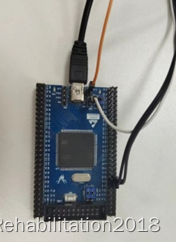
DE1-SOC The working frequency of the development board is 50Mhz, chart 4-2 Middle box 1 Indicates the key , Used to deal with FPGA Module initialization ; Square box 2 Express LTC2308 Connect the signal source ; Square box 3 Express VGA Connect the monitor .

chart 4-3 The experimental result is that the clock frequency of the development board is 10KHz,VGA The clock frequency of is 25MHz In the case of . In this case of clock frequency allocation , The display shows the waveform by scanning left and right . And when observing experimental phenomena , The display will intermittently display the waveform .
Cause analysis ,VGA Of 25MHz Get the development board under the clock frequency 10KHz Processing the data , In this condition ,VGA After displaying a set of pixel data , We need to wait for the development board to process the next group of waveform data . If you adjust the clock frequency of the development board to 25MHz perhaps 50MHz, be VGA Unable to accurately receive pixel data , The black screen will appear on the display .
However , By calling VGA_controller and DMA etc. IP nucleus , Will be used to solve the problems encountered above , The experimental results are shown in Fig 4-4 Shown .DMA(Direct Memory Access, Direct memory access ), It allows hardware devices of different speeds to communicate , Without the need for CPU Large amount of interrupt load .
PIO In mode, the data transmission between hard disk and memory is controlled by CPU Controlled ; And in the DMA In mode ,CPU Just ask DMA The controller commands , Give Way DMA Controller to handle the transmission of data . And in DMA In mode , There is SRAM And FIFO etc. IP nucleus , Play a DMA And the buffer between peripheral devices or memory .
IP nucleus VGA_contronller The display scanning mode that can be set is up and down scanning .
5、 ... and 、 Tool use
5.1 Using logic analyzer and Modelism
Use Modelism Yes FPGA The module is simulated , To understand FPGA The state machine of the module .
chart 5-1 In the test file , By reading the waveform data designed by yourself and CFG Configuration information , And rely on multiple test ports (test1、test2、test3) To detect FPGA Changes of state machine and key parameters in the module , With this full understanding verilog The design framework of the program .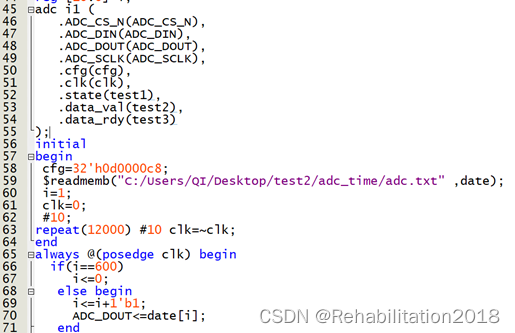
Use logic analyzer to analyze FPGA The module detects the state machine and port changes during the operation of the development board , It is convenient to screen out the error position of waveform data .
For detailed steps, please refer to the corresponding video link below .
https://www.bilibili.com/video/BV1o54y1L7ut?vd_source=bf69d71b17066eefdcd36c6207919226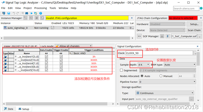
5.2 Make embedded linux-SD System startup card
Realize the function of oscilloscope software , need linux The system goes through linux-SD System startup card control development board ARM chip , achieve FPGA and ARM The combined application of .
about linux-SD Production of system startup card , Need to be in SD Card a2、ext3 and fat3 Partition , Prepare the following documents , Please refer to the production process SoC-FPGA Design Guide DE1-SoC Edition.pdf Of the 13 Chapter and chapter 11.1 chapter .
sdcard/
├── a2
│ └── preloader-mkpimage.bin
├── ext3_rootfs.tar.gz
└── fat32
├── socfpga.dtb
├── socfpga.rbf
├── u-boot.img
├── u-boot.scr
└── zImage
adopt linux Systematic minicom Terminal control DE1-SOC equipment , Pictured 5-3 Shown .
5.3 Study HPS and FPGA Address mapping for
Map the physical address of the memory in the development board to the virtual address that the application software can access , You need to do the following .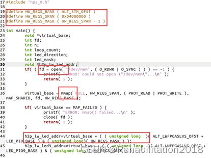
First ,open Open the memory device driver through system call " /dev/mem ".
then mmap Through system call, it is used to put HPS The physical address is mapped to void Pointer to the variable virtual_base Represents the virtual address of . The code converts the physical base address of the peripheral area (HW_REGS_BASE = 0xfc000000) Map to a virtual address based virtual_base. For any peripheral area controller , The user can use its offset relative to the peripheral area and the virtual address based on virtual_base Stack to calculate the virtual address of the controller of any peripheral area .
For detailed operation steps, please refer to the corresponding documents in the following links .
https://blog.csdn.net/liluxiang333/article/details/113626965
5.4 Connect the computer with the development board NFS Mount
Connect the computer and the development board through the network cable , It is convenient to put the executable file obtained from the software code into SD Card execution .
Operation steps :
First step
https://blog.csdn.net/thisway_diy/article/details/111474111
The second step
Ensure that the development board can ping through Ubuntu
minicom terminal Use ifconfig command
Automatically :inet addr:10.42.0.98 ( Development board IP)
Terminal use hostname -I
There are two IP Namely ubuntu Development board
Use ping Make sure the development board and ubuntu It can transmit signals
The third step
stay minicom Terminal mount
https://blog.csdn.net/LMmcu_2012/article/details/78566067
Step four experimental result 
Step five Cancel the mount
sign out minicom terminal
6、 ... and 、 Problems in the direction of the design process
(1) face ARM and FPGA Combined applications , First you should find a routine , Use routines to quickly understand the problem of address mapping ;
(2) Ignore the scope of use of logic analyzer tools ;
(3) Too entangled oscilloscope text information compilation problem .
边栏推荐
- AcWing 92. 递归实现指数型枚举
- What is prescaler in STM32
- Quick check list of various XSS payloads
- GCC的基本用法
- Linked list - Sword finger offer interview question 02.07. linked list intersection
- [markdown grammar advanced] make your blog more exciting (IV: set font style and color comparison table)
- 08.01 adjacency matrix
- L1-043 reading room
- Literature record (part109) -- self representation based unsupervised exemplar selection in a union of subspaces
- Qt5.12 + vs2019 cannot locate the program input point in the dynamic link library
猜你喜欢
QT notes - qtablewidget table spanning tree, qtreewidget tree node generates table content

Cgo+gsoap+onvif learning summary: 9. Go and C conduct socket communication and onvif protocol processing

Basic usage of GCC

The art of management - driving software R & D efficiency through leadership

Miss waiting for a year! Baidu super chain digital publishing service is limited to 50% discount
字符串匹配的KMP
![MOS tube - Notes on rapid recovery application (I) [principle]](/img/a1/8427c9b1d0ea0cecce820816510045.png)
MOS tube - Notes on rapid recovery application (I) [principle]

源码分析Sentry用户行为记录实现过程

在kuborad图形化界面中,操作Kubernetes 集群,实现mysql中的主从复制
![Detailed OSPF configuration of layer 3 switch / router [Huawei ENSP experiment]](/img/a9/f080940ec7bf94ab83c922990efa62.png)
Detailed OSPF configuration of layer 3 switch / router [Huawei ENSP experiment]
随机推荐
Repeated calls, messages, idempotent schemes, full collation
Skillfully using command line parameters in Delphi to realize the trigger function of dragging files onto program icons
Day4: circular structure
4*4图片权重的收敛规则
CCF 201803_ 1 jump jump
MES系统设备管理概述(中)
C language programming code
Shell script
[rust] what software should I use to develop rust? Recommended editors commonly used to support rust
AcWing 92. 递归实现指数型枚举
SQL multi condition query cannot be implemented
What is prescaler in STM32
Types and history of bugs in it circle
Use of multithreading in QT
The difference between synchronized and lock locks
Microservice - eruka
L1-043 阅览室
Markdown mathematical formula syntax
三层交换机配置MSTP协议详解【华为eNSP实验】
Qt5.12 + vs2019 cannot locate the program input point in the dynamic link library