当前位置:网站首页>MOS tube - Notes on rapid recovery application (I) [principle]
MOS tube - Notes on rapid recovery application (I) [principle]
2022-07-24 11:25:00 【It is said that this is ZZY】
MOS tube —— Quick recovery application notes [ Principles ]
The next article : Please open this column
The content of this article is MOS The opening content of the tube , Help you understand and use the structure MOS tube .
List of articles
- MOS tube —— Quick recovery application notes [ Principles ]
- The working principle of field effect transistor
- Differences and advantages between FET and bipolar transistor
- Classification and schematic definition of FET
- Principle and structure of FET
- NMOS The internal structure of
- The principle of metal oxide effect
- Gold oxygen effect and MOS Structural coordination
- MOS Real structure and parasitic diode
- MOS Working mode of
- Cut off zone ( Subthreshold region or weak inversion region )(cutoff, subthreshold or weak-inversion mode)
- Linear area ( Three pole region or ohmic region )(linear region, triode mode or ohmic mode)
- Saturation zone ( Zoom in )(saturation or active mode)
- MOS The symbol of the tube
- NMOS
- PMOS
The working principle of field effect transistor
Field effect tube (Field Effect Transistor —— FET) It's a unipolar transistor , And bipolar transistors BJT All belong to transistors (Transistor). In bipolar transistors , Carriers include electron motion and hole motion , Flow to both poles like a double force ; And in the field effect tube , There is only one carrier motion , Or electrons or holes , Flow to one pole , Therefore, it is called unipolar transistor .
Differences and advantages between FET and bipolar transistor
Although unipolar type was born relatively late , But through its inherent advantages , Such as low noise 、 High resistance and low power consumption 、 Good thermal stability, etc , At the same time, both of them can realize amplification function and switching function , So it was rolled directly BJT, Its invincible low power consumption is favored by the field of digital chips , As the times change ,MOSFET Basically completely replaced BJT, Only in some simulators, such as : Operational amplifier 、 A / D converter 、 Power module 、 UHF 、 Current amplification 、 Low cost applications BJT It also accounts for a certain proportion .
Classification and schematic definition of FET
FET can be roughly divided into the following two types :
The junction field effect working current is very small , Suitable for analog signal amplification , It is divided into N Channel and P Two kinds of ditches . Like in bipolar transistors NPN and PNP equally ,M Channel and P The channel is just the opposite direction of the working current . Junction FET has limited applications , The small number . It's not detailed here , Only to understand .
MOSFET Classification and classification of BJT It's not nearly the same ,MOSEFT As the most common FET First, it is divided into two types: enhanced type and exhausted type , Under the two types, it can be divided into N Channel and P Ditch .
Of course, there are also some ways to distinguish according to the working voltage and current , It is generally divided into small signal tube and power tube .
Principle and structure of FET
Want to really understand MOS How it works, we must know its physical structure , The content of most books is not clear , Today, let's summarize what I know . The following is all about enhanced , Because there are few exhausted models , The difference between the two will be explained by the way below .
NMOS The internal structure of
Here is a N type MOS Section of , Let's explain in detail through the sectional drawing .
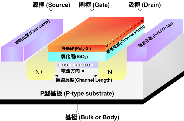
It can be seen that he uses a piece with relatively low doping concentration P Type silicon chip as substrate , Using the diffusion process, two highly doped N Type area .
NMOS Marked on the source and drain of “N+” It represents two meanings :
(1)N Represents doping (doped) The polarity of impurities in the source and drain regions is N;
(2)“+” It represents that this region is a region with high doping concentration (heavily doped region), That is, the electron or hole concentration in this region is much higher than that in other regions . The source and drain are separated by a region of opposite polarity , That is, the so-called base ( Or matrix ) Area . If it is NMOS, Then the doping of the matrix region is p-type. The opposite is true of PMOS for , The substrate should be n-type, And the source and drain ( The image above Drain) Then for p-type( And it is highly doped P+). The doping concentration of the substrate does not need to be as high as the source or drain , Therefore, there is no “+”, As a channel .
You can see in the N Two ohmic electrodes led out of the A-type region , They are called sources (Source) And the drain (Drain), In order to simplify symbol writing, we often use S and D To represent the above electrodes respectively .
You can notice that the upper layer of the lead out electrode is not completely empty , Instead, there is an oxide film , The corresponding figure above is the field oxide (Filed Oxide), The material of oxide layer is mostly silicon dioxide , Below it is the base silicon , And the top is used as a grid polysilicon , Of course, in the early days, polysilicon here was replaced by aluminum electrode , And lead it out. This is the grid (Gate). When the oxide layer covered by the upper layer was metallic aluminum in the early days , People usually call this structure metal oxide effect tube , This is also MOS The origin of the name .
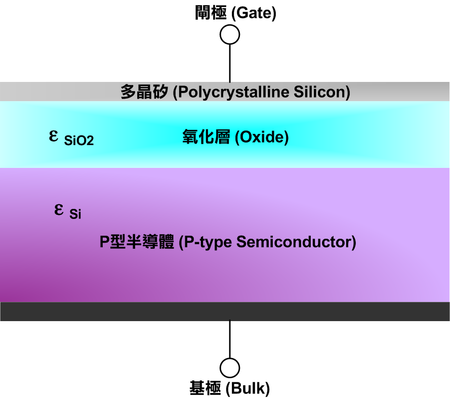
The principle of metal oxide effect
MOS The tube is structurally represented by a Metal — Oxide layer — semiconductor ( The base ) Of capacitance At the core , The material of oxide layer is mostly silicon dioxide , Below it is silicon as a base , On top of it is polysilicon as a gate ( In the early days, it was metal ). Such a structure is exactly equal to a Capacitor . The oxide layer is in the capacitor Dielectric , The capacitance value is determined by the thickness of oxide layer and that of silicon dioxide Dielectric coefficient To decide . Gate polysilicon and base silicon Then become MOS The two ends of the capacitance . The complete structure is as follows :
Accumulation stage
When a voltage is applied to MOS At both ends of the capacitor , The charge distribution of semiconductors will also change . As shown in the figure below :

In this picture , Blocks with different oxide thickness are shown p Type substrate MOS-CAP Of C-V curve . The displayed blue curve refers to high frequency C-V curve , The red curve refers to low frequency C-V curve . In the accumulation and depletion stage ,MOS Capacitance is independent of all frequencies . It's because here , The total charge is controlled by most carriers . In the inversion area , The charge is dominated by a few carriers , Form inversion layer . Because the time of minority carrier generation is limited , At higher frequencies , The total charge cannot follow the gate bias , This can lead to C-V The difference in the curve . It is also worth noting that the threshold voltage changes with different oxide thickness .
Capacitance formula high speed our capacitance is only related to dielectric constant, thickness and area , So it has nothing to do with voltage . however MOS The capacitance of the structure will change with the change of voltage , So we went through C-V Curve to analyze , Because the substrate is P, And the accumulation is P-type, So the lower electrode just has better conductivity , All grid voltages are applied to G On , So at this time, the capacitance is the largest .
exhaustion phase
contrary , When a positive voltage VGD Applied to the grid and base terminals ( Pictured ) when , The concentration of holes will decrease ( It is called exhaustion , Such as C-V In the middle of the curve ), Electronics The concentration of will increase .
Inversion stage
When VGB When strong enough , The electron concentration close to the gate extreme will exceed the hole . This is in p-type In semiconductors , Electron concentration ( With a negative charge ) Beyond the hole ( With a positive charge ) Area of concentration , It's called Reverse layer (inversion layer).
In the inversion zone , That is to say Vg When it is greater than the opening voltage , At this time, the width of the depletion region reaches the maximum , So enter strong inversion , At this time, the capacitance reaches the minimum . Of course, there is also a problem that cannot be ignored is the frequency of our test voltage , When the frequency is low , The velocity of carriers can follow the change of voltage and frequency , So at this time, the inversion region is charged and finally reaches GOX The thickness of the . And if it's high frequency , The carrier speed cannot catch up with the charging speed of the inversion region , So it can only be kept in a low capacitance state . In fact, the width of the inversion region is closely related to the substrate concentration ( This may use Vt And substrate concentration , Therefore, the change of substrate concentration can be judged by the high-frequency capacitance characteristics of the inversion region .
MOS The characteristics of the capacitor determine the working characteristics of the MOS half effect transistor , But a complete MOS half effect transistor structure still needs a supply Most carriers (majority carrier) And the drain that accepts these most carriers .
Gold oxygen effect and MOS Structural coordination
MOS Real structure and parasitic diode
In theory , One MOS The package of should have four legs , Source pole (S)、 Drain electrode (D)、 Grid (G) Outside , There is still one The base (Bulk or Body), For example, as shown below :

But in fact, they are sold on the market MOS The structure is not like this , It should be as follows :

This is because the base and source are usually connected , As shown in the symbol above , Therefore, distributed MOS FETs are usually three terminal devices . In integrated circuits, metal oxide half effect transistors usually use the same base (common bulk), Therefore, the polarity of the base is not marked , And in the PMOS Add an extra circle at the extreme of the grid to show the difference .
Put the substrate, that is B and S What will happen if they are connected ?
Please look at the chart below. :

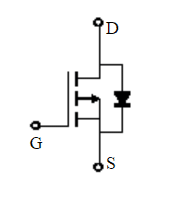
This is a NMOS, When the substrate and S When connected, it will be like the above , here S To D The passage of will form a magical thing :PN junction , As shown below :

in other words , When we are directly on NMOS have to S and D When a voltage is applied to the pole , He will directly connect . And we call this formed diode Parasitic diode . This is from MOS Structurally determined , Is inevitable .
You may not believe it , Let's test it through simulation , The circuit structure is as follows :

The simulation results are as follows :

Let's change the circuit structure , have a look DS Whether it is still conductive ? The changed structure is as follows :

give the result as follows , Sure enough, it doesn't work .

Here we need to explain : Field effect tube (JEFT No MOS) in , The source and drain are symmetrical , interchangeable . But in MOSFET in , Because the substrate and source have been connected internally , Even a lot MOSFET The interior is still D、S A diode is connected in parallel , Note that a diode is really added here, not a body diode , therefore D and S Not interchangeable .
MOS Working mode of
According to in MOS The grid of the tube 、 Source pole , Applied by three endpoints such as drain bias (bias) Different , The MOS half effect transistor will have the following three operating modes .
Cut off zone ( Subthreshold region or weak inversion region )(cutoff, subthreshold or weak-inversion mode)
When ∣ V G S ∣ < ∣ V t h ∣ |V_{GS}| < |V_{th}| ∣VGS∣<∣Vth∣ when :
∣ V G S ∣ |V_{GS}| ∣VGS∣ Represents the bias difference from grid to source ( Voltage difference ), ∣ V t h ∣ |Vth| ∣Vth∣ Of materials Critical voltage , That is, the voltage when the above gold oxygen effect reaches the inversion . This MOS half effect transistor is in end (cut-off) The state of , The channel remains P Disconnected state , There are not enough majority carriers , Current cannot flow through this MOS tube , That's it MOS The tube doesn't work .
here MOS The state is as follows :

It can be seen that the designated area has not formed a passable area , It is a depletion region formed by the substrate and the doped region (depletion region), At this time, no current can pass .
Linear area ( Three pole region or ohmic region )(linear region, triode mode or ohmic mode)
When V G S > V t h V_{GS} > V_{th} VGS>Vth And V G D > V t h V_{GD} > V_{th} VGD>Vth when :
here VDS by NMOS Voltage from drain to source , Then this one NMOS For the condition of conduction , Channels under the oxide layer have also been formed . Now this one NMOS The behavior is similar to that of a voltage controlled resistor (voltage-controlled resistor), The current flowing from the drain to the source is :
I D = μ n C o x W L ( V G S − V t h − V D S 2 ) V D S I_{D}=\mu_{n} C_{o x} \frac{W}{L}\left(V_{G S}-V_{t h}-\frac{V_{D S}}{2}\right) V_{D S} ID=μnCoxLW(VGS−Vth−2VDS)VDS
μn Is the carrier mobility (carrier mobility)、W Is the gate width of the MOS half effect transistor 、L Is the gate length of the MOS half effect transistor , and Cox Is the unit capacitance of the gate oxide . In this area , The current of the MOS half effect transistor — The voltage relationship is like a linear equation , So it is called linear region .
When working in a linear region MOS The solution diagram of is as follows :

You can see that the inversion layer appears in the corresponding area , Now S and D In between Channel.
The following figure shows NMOS Drain current of I D S I_{DS} IDS And drain voltage V G S − V t h V_{GS}-V_{th} VGS−Vth The relationship between :

You can see that with V G S − V t h V_{GS}-V_{th} VGS−Vth The current that can be passed by the change of also continues to increase , Until the current that can pass through a certain voltage value does not change , This voltage value is what I want to say below Saturation zone ( Zoom in ).
Saturation zone ( Zoom in )(saturation or active mode)
When $V_{GS} > V_{th} $ V G S Keep a certain V_GS Keep a certain VGS Keep a certain And V G D < V t h V_{GD} < V_{th} VGD<Vth when :
this Mos The tube is in the condition of conduction , It also forms a channel for current to pass . But with the drain voltage (D) increase , When the grid voltage is exceeded , It will make the charge of the inversion layer close to the drain region zero , The channel here almost disappeared ( Here's the picture ), This situation is called Pinch off (pinch-off).

Be close here D The channel of the pole has disappeared . The following figure shows more clearly .

In this case , When the carrier from the source reaches the pinch point through the channel , Will be injected into the space charge region around the drain (space charge region), Then it is swept into the drain by the electric field . At this time, the current passing through the MOS half effect transistor and its drain — Voltage between sources VDS irrelevant , Only related to grid voltage , The main reason is that the gate voltage near the drain region is not enough to reverse the channel , As a result, the available carriers are limited , It limits the current of the channel , The relationship is as follows :
I D = μ n C o x 2 W L ( V G S − V t h ) 2 I_{D}=\frac{\mu_{n} C_{o x}}{2} \frac{W}{L}\left(V_{G S}-V_{t h}\right)^{2} ID=2μnCoxLW(VGS−Vth)2
The above formula is also ideal , The relationship between current and voltage of MOS half effect transistor working in saturation region . In fact, in the saturated zone MOS The drain current of the tube will be due to Channel length modulation effect And change , Not with VDS It has nothing to do with . Saturation current after considering channel length modulation effect — The voltage relationship is as follows :
I D = μ n C o x 2 W L ( V G S − V t h ) 2 ( 1 + λ V D S ) I_{D}=\frac{\mu_{n} C_{o x}}{2} \frac{W}{L}\left(V_{G S}-V_{t h}\right)^{2}\left(1+\lambda V_{D S}\right) ID=2μnCoxLW(VGS−Vth)2(1+λVDS)
We don't consider here MOS Amplification of , Give priority to switching function , Wait until you explain the amplification circuit .
The following figure shows a N Ditch MOS Transfer characteristics and output characteristics of the tube .

The so-called transfer characteristic refers to the constant V D S V_{DS} VDS Under different conditions V G S V_{GS} VGS Voltage conditions can output current electric size , That is, it corresponds to the saturation current in the saturation region above , It should be emphasized that the channel is not completely clamped off in the saturation zone , Just because of the limitation, the current cannot rise any more , That is, the red part corresponding to the above figure and the left figure .
The output characteristic diagram is the figure on the right ,MOS When the tube is used as a switch, it works in the saturation zone , By controlling GS Between a certain value and 0V To switch between on and off .
In order to understand the switching in different areas , I found the following figure :

among $V_{\mathrm{DS \underline{}} \mathrm{dv}}=V_{\mathrm{GS}}-V_{\mathrm{GSTH}} $, In essence, it is the intersection of the red curve and the right curve in the above figure .
MOS The symbol of the tube
The following figure shows the common enhanced mos The symbol of .

Generally, we don't discuss depletion , Only enhanced .
NMOS

This is P In the ditch MOS Pipe symbol diagram , According to the above, we know P In the ditch MOS The base of is N Type semiconductor , The arrow in the figure above actually indicates when the body diode is on , Flow direction of current , This is from D To S. meanwhile GS The voltage is opposite to the corresponding conduction direction , in other words GS The voltage is less than 0 It can be connected normally when .$V_{GS} < 0 $.
Of course, the pictures given by some manufacturers are also very direct , Here's the picture :
This directly indicates the corresponding diode , But generally, this kind of diode is really encapsulated , Not a body diode , Here we need to pay attention to .
PMOS
This is N In the ditch MOS Pipe symbol diagram , According to the above, we know N In the ditch MOS The base of is P Type semiconductor , The arrow in the figure above actually indicates the conduction direction of the body diode , It is explained here that the voltage is directly applied at SD It can be connected , Of course GS The conduction can be realized only when the voltage meets the following :$V_{GS} > 0 $.

Of course, the pictures given by some manufacturers are also very direct , Here's the picture :

Reference article :
边栏推荐
- 【C】 Understanding C language variable scope and life cycle from memory
- 强引用、软引用、弱引用、虚引用有什么区别?
- Blue Bridge Cup - binary conversion exercise
- 简单使用 MySQL 索引
- HCIP MGRE实验 第三天
- Blue Bridge Cup provincial match training camp - Calculation of date
- JMeter接口测试步骤-安装教程-脚本录制-并发测试
- Fiddler packet capture tool summary
- 运算放大器 —— 快速复苏笔记[贰](应用篇)
- [golang] golang implements the URLEncode URLDecode function
猜你喜欢

Ask n! How many zeros are there behind

性能测试总结(一)---基础理论篇
What is cloud native? Why is cloud native technology so popular?

Lanqiao cup provincial training camp - stack and recursion

Talk about software testing - automated testing framework
Performance test summary (I) -- basic theory

【Markdown语法高级】让你的博客更精彩(四:设置字体样式以及颜色对照表)

自学软件测试天赋异禀——不是盖的

Imeta view | is short reading long amplicon sequencing applicable to the prediction of microbiome function?

Lanqiao cup provincial training camp - commonly used STL

随机推荐
性能测试总结(一)---基础理论篇
In BS4.String and Difference between text
ctfshow ThinkPHP专题 1
Robot framework official tutorial (I) getting started
基于NoCode构建简历编辑器
HCIP MGRE实验 第三天
【反序列化漏洞-02】PHP反序列化漏洞原理测试及魔术方法总结
Directional crawling Taobao product name and price (teacher Songtian)
Stm32+esp8266+mqtt protocol connects Alibaba cloud Internet of things platform
The third day of hcip mGRE experiment
Leetcode 112. 路径总和
Stack Title: basic calculator II
[golang] golang implements the post request to send form type data function
Semaphore详解
E2PROM read / write (xiicps) on PS side of zcu102 board
Ask n! How many zeros are there behind
HCIP OSPF接口网络类型实验 第四天
Over the weekend, I had a dinner with the technology gurus and talked about the "golden nine and silver ten" peak of the software testing industry [the trend of involution has been formed]
Fiddler抓包工具总结
这个应该是全网最全的接口测试工具之postman