当前位置:网站首页>[sequential logic circuit] - register
[sequential logic circuit] - register
2022-07-24 07:15:00 【Li Yuchen】


Welcome to learn digital circuit —— Sequential logic circuit .
Here we will explain the digital register 、 shift register 、 Unidirectional shift register and integrated bidirectional shift register 74LS194, I hope that through our study, you will better understand the mystery of digital circuits .
Catalog
(3) Analysis of digital registers
(1) Unidirectional shift register
(2) Integrated bidirectional shift register
①74LS194 The physical object and pin arrangement of the chip
②74LS194 The logic function of the chip
One 、 register
In digital circuits , It is often necessary to store data or calculation results temporarily . A circuit that can temporarily store binary data is called register . It consists of a trigger with memory function and a gate circuit . A trigger has only 0 and 1 Two states , Can only store 1 Bit binary code ,n Triggers can be formed to store n Bit binary register . In the clock pulse CP Under control , The register receives the input binary number and stores it . According to different functions , Registers can be divided into Digital register and shift register .
1. Digital register
The digital register has receive 、 Storage and Clear the original data The function of .
(1) Circuit composition
As shown in the figure is a basic RS Trigger and gate circuit 4 Logic circuit diagram of bit digital register .4 individual RS The reset end of the trigger is connected together , As the zeroing end of the register  ,
, Is the data input of the register ,
 Is the output of data .

(2) working process
The work of register is divided into two steps :
① Clear the register first
Add a negative pulse at the reset end before receiving data ( Reset pulse ), Set all triggers 0, After the reset pulse returns to the high level , Prepare for receiving data .
② Receive pulse control data storage
Receive pulse CP( Positive pulse ) arrival , Will NAND gate G0~G3 open , Receive input numbers  . for example , if =1101, be G3、G2、G1、G0 Output is 0010, Each trigger is set to 1101, namely


 =1101, Complete receiving and deposit .
It can be seen that , The above registers are in operation , Input all numbers at the same time , And output all numbers at the same time , This digital input 、 The output mode is Parallel input 、 Parallel output The way .
(3) Analysis of digital registers
advantage : Short storage time 、 Fast .
shortcoming : After power failure , All the stored numbers are lost .
2. shift register
Shift registers can not only register numbers , It also has a shift function . Shift means that under the control of shift pulse , Trigger left or right adjacent bits in turn transfer digital processing .
The shift register is divided into Unidirectional shift register and Bidirectional shift register .
(1) Unidirectional shift register
① Circuit composition
As shown in the figure, it is JK The trigger consists of 4 Bit unidirectional right shift register . Of each trigger in the figure J、K Both ends are connected with the adjacent lower trigger  、
、 End connection , The lowest one on the left JK trigger FF0 Of K Connect a non gate in series at the end, and then connect with J End to end , As the input of receiving external data , each JK Trigger J And K Always in the opposite state , send JK Trigger only has set 0 Harmony 1 The function of . The shift control signal is added to the... Of each trigger at the same time CP End .

② working process
stay CP Under the action of falling edge , The number to be stored is sent to FF0, The status of other triggers is the same as CP The moment before the action is low 1 The state of the bit trigger is the same , That is, the original number in the register is shifted to the right once 1 position .
Next, save the number 1011 For example , analysis 4 Working process of bit shift right register , To deposit digital =1011, Generally, register first clear 0, Then the stored number will be changed from high to low According to the shift pulse beat, it is sent to  End , When the first One CP When the rising edge comes =1, be =0001; When the second CP When the rising edge comes ,=0,=0010, After four shift pulses, the register status is =1011. As shown in the figure :

(2) Integrated bidirectional shift register
①74LS194 The physical object and pin arrangement of the chip
As shown in the picture 74LS194 The real chip and its pin arrangement :

It is a parallel data input ; Is the right shift serial data input ,
 Is the left shift serial data input .
Is the register parallel data output .
 and
and  It is the control end of bidirectional shift register .
②74LS194 The logic function of the chip
As shown in the figure :
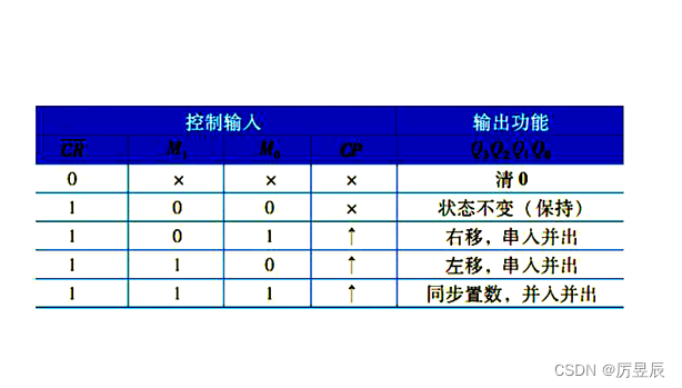
It can be seen from the table that ,74LS194 The chip has the following logic functions :
Keep function : When ==0 when , With or without CP When it works , The contents of the register remain unchanged .
Parallel number setting function : When = =1 when , stay CP When the rising edge acts , Send the numbers at the data input side to the register in parallel , send =.
Shift right function : When =0、=1 when , In the shift control signal CP When the rising edge acts , The numbers in the register are shifted one bit to the right , And will Deliver to .
Move left function : When =1、=0 when , stay CP When the rising edge acts , The digits in the register are shifted one bit left in turn , And will Deliver to .
Asynchronous reset function : When =0 when , Clear directly , Register bits () Are all 0, You cannot set numbers and shift . Only when =1 when , Registers allow operation .
The next article continues to explain counters 🥰🥰
边栏推荐
- Don't care too much about what others think of you
- Ue4/5 cannot open the file "xxx.generated.h" (cannot open file xxx.generated.h) solution summary
- Can recursion still play like this? Recursive implementation of minesweeping game
- Lambda expressions sort list objects in multiple fields
- Unity中使用深度和法线纹理
- 处理树形结构数据
- 找工作备忘
- 一个怎样的模式能让平台用户发生自助裂变?-链动2+1
- 变量和数据类型(03)
- Redis fragment cluster
猜你喜欢

Filter filter

Redis 主从机制

One book a day: machine learning and practice -- the road to the kaggle competition from scratch
Redis master-slave mechanism

周杰伦直播超654万人观看,总互动量破4.5亿,助力快手再破纪录

"Big factory interview" JVM Chapter 21 questions and answers
Chapter007 FPGA learning IIC bus EEPROM reading

文件上传下载Demo

17. What is the situation of using ArrayList or LinkedList?

【LeetCode-简单】20. 有效的括号 - 栈
随机推荐
C language to achieve three chess? Gobang? No, it's n-chess
C language from entry to soil (I)
Part II - C language improvement_ 3. Pointer reinforcement
Upload pictures Base64
传统电商红利消失,怎么进军新型社交电商?
Huawei experts' self statement: how to become an excellent engineer
C language from entry to soil function
JMeter notes 2 | JMeter principle and test plan elements
Part II - C language improvement_ 2. Memory partition
17. 什么情况用ArrayList or LinkedList呢?
被马斯克热炒的人形机器人Optimus“擎天柱“,中国厂商或后来居上
Accumulation of project problems
C language from introduction to soil -- super detailed summary of operators
Chapter007-FPGA学习之IIC总线EEPROM读取
重磅直播 | ORB-SLAM3系列代码讲解地图点(专题二)
The function of extern, static, register, volatile keywords in C language; Nanny level teaching!
GIMP自定义截图
Input the names of 10 people and output them in descending order
上传excel文件
【Word】如何生成左侧的索引目录