当前位置:网站首页>From A76 to A78 -- learning arm microarchitecture in change
From A76 to A78 -- learning arm microarchitecture in change
2022-07-24 22:07:00 【Kernel craftsman】
One 、 introduction
With the rapid development of smart phones , Mobile processor architecture designer ARM The company updates almost every year CPU The core structure of . from 2018 to 2020 year ,ARM The company is based on ARMv8 The architecture has launched three generations Cortex-A76、Cortex-A77、Cortex-A78 classic CPU Core architecture . Based on these generations CPU framework , Chip design manufacturers have also designed a number of processor products with excellent performance . This paper starts from A76 Microarchitecture begins to learn , By comparing the changes of each generation , Let readers understand the key knowledge of processor microarchitecture . The following table gives some information based on these three generations ARM Typical processor products of processor architecture .

Two 、 from A76 Begin to understand ARM Microarchitecture
from ARM Of A76 Start , More information can be found on the network , For example, we can start from wikichip Website (en.wikichip.org) Get A76 Complete microarchitecture block diagram .

1. DSU(DynamIQ Shared Unit)
from A75 Start ,ARM A new multi-core management system unit is proposed , be called DSU. adopt DSU modular ,CPU Designers can place and share the cores of different architectures at will L3 cache , Reduce the loss of data directly transmitted by different architecture cores . stay DSU Before the architecture , Every Cluster It needs to be placed in the same structure CPU, Such as the 4 individual A73 The processor is placed in a Cluster in , take 4 individual A53 Put it on another Cluster in , these two items. Cluster There will be a certain connection loss in the mutual access of data .

utilize DSU modular , Developers can design at will CPU The combination of , For example, in the figure 1 Big +7 Small ,2 Big +6 Small ,4 Big +4 Small ,1 Big +2 Small ,1 Big +3 Small ,1 Big +4 Small and so on .

2. Performance and power consumption optimization

Architecture and process have certain relevance , Such as A76 Architecture design can adopt 7nm process , according to ARM data , be based on 7nm Of A76 Bi Ji Yu 10nm Process of A75, Performance can be improved 40%, Or reduce energy consumption under the same energy 50%. so A76 Compared with the previous generation A75 It's a big improvement , Later, we will learn more about the differences in architecture .
3. Third level cache design
A76 Adopt three-level cache mechanism , among :
L1 Is the core unique cache , Having independent 64KB Instructions Cache(ICache) and 64KB data Cache(DCache);
L2 Is the core unique cache , It can be configured as 256KB perhaps 512KB( Add money );
L3 Shared cache between cores , stay DSU Inside , It can be configured as 2MB perhaps 4MB.
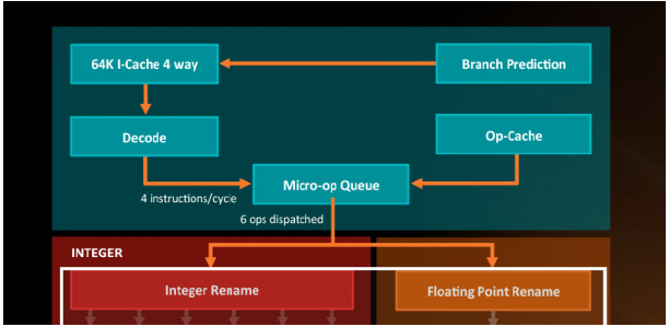
4. Branch prediction unit (BPU)

In multistage pipeline system , When executing the branch judgment instruction , If the system doesn't know which branch to take , You need to wait until the branch execution results before you can get the correct instructions . To improve pipeline performance , Modern processors provide a branch prediction unit (BPU), Used to predict common paths , And prefetch instructions in advance , Ensure that the assembly line is filled completely .
A76 Of BPU And instructions Fetch Unit independent ,BPU Can be at the same time with Fetch Unit work , Speculate in advance and get post branch instructions , Reduce the delay of branch prediction .
5. Front end design (Front-end)

After instruction prefetching, it enters a decoding queue ,A76 Provides 4 road decoder, comparison A75 Added all the way decoder unit , This is an element of performance improvement .
6. ROB Module design

The decoded instructions are called MOP(Macro-Operation),MOP Not actually executed instructions , The instructions finally sent to the execution unit are called uOP(Micro-Operation).MOP Than uOP A little more complicated , It could be more than one uOP Combined instructions , Through the disassembly of the rear end unit , You can put MOP Decompose into the most basic instructions that the processor can execute uOP,uOP The number of instructions is about MOP many 20%.
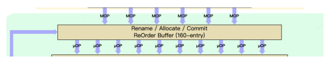
ROB(ReOrder-Buffer) The module provides 128 individual entry, Used to reorder instructions , Fill the assembly line as much as possible , Here you can see A76 The input of the design is 4 road MOP, The output is 8 road uOP.
7. execution unit (Execution Engine)

Dispatch Unit will uOP Instructions are sent to the execution unit (Issue), The execution unit provides 120 individual entry, Divided into three categories : integer 、 Floating point and read / write , The integer part includes 1 Branch units ,2 A foundation ALU unit ,1 Compound ALU unit ; Floating point section provides 2 individual 128bit Advanced SIMD Instruction unit ; The reading and writing section provides 2 individual AGU(Adress Generation Unit) Address unit .
8. LSU(Load Store Unit) Design

LSU Modules and execution units 2 individual AGU Connect , Simultaneous connection 64KB Of L1 Data caching (DCache), And provide 2 individual 16B/cycle Of load Port and 1 individual 32B/cycle Of store port .
9. Summary
thus , We take the finger 、 decoding 、 Instruction dispatch 、 Command launch 、 Instruction execution to data reading and writing , A brief understanding A76 Processor microarchitecture , In the next section, we will compare A77 and A76 Differences in Architecture , Learn more ARM The pace of microarchitecture design .
3、 ... and 、A77 Microarchitecture and A76 contrast
A77 Micro frame composition , Let's look at it and cherish it , Because self A77 After that, it is difficult to find a complete micro frame composition on the network .

1. Performance improvement

ARM The data shows that it is also 7nm process 3GHz Under the condition of ,A77 The performance is comparable to A76 promote 20%, Note that it is marked with single thread performance improvement , Later, we can infer the reasons for the performance improvement from the architecture upgrade .
2. L0 cache (MOP Cache)

A77 New introduction MOP Cache modular , This module is not ARM Innovative design , stay PC The processor already has , for example Intel In the early days of core Sandy Bridge Added to the processor uOP Cache modular .

Besides AMD Of Zen Architecture also has MOP Cache module .
MOP Cache Mainly for L0 Level cache , Store decoded MOP Instructions .MOP Cache The advantage is that if you find the required instructions in it , The front circuit modules can be temporarily controlled by MOP Cache To replace , It can save power and improve performance .ARM The data shows this MOP Cache The hit rate is 85%, It can be seen that A77 A very big improvement of .
Continue to look at MOP Cache The size of the ,ARM The dimension data given is 1.5K instead of 1.5KB, The unit is not Byte But a piece , in consideration of ARM routine decoded The machine code is 32 A wide (Aarch64 It's also 32 A wide , Of course, there are individuals 64 Bit width instruction ), Guess this L0 Cache The size of the should be 6KB about ( and Intel Of sandy bridge At the same ).
Mobile processors are introduced L0,ARM Not the first , As early as Qualcomm Snapdragon S4 The times are here Krait The core introduces L0 cache. Display according to data 1.5K Of Cache You can achieve 80-85% shooting , add Cache, The marginal effect of improving the hit rate will become more and more obvious .
3. Front end design (Front-End)

A77 be relative to A76 Another important change is to produce MOP The ability to command from the original per cycle 4 Up to 6 individual , however decode The ability to keep 4 There is no change . You can compare the whole fetch and decode The basic structure and A76 No big change ,MOP The main reason for promotion is the new MOP Cache Provided . If MOP Cache hit , To bypass decode Modules can be fetched at most once 6 strip MOP Instructions , If you don't hit back decode The module is still one time 4 strip ,L0 Cache and Decode Made a good supplement , Let one cycle provide more MOP Instructions .
4. ROB Module design
A77 relative A76 The size of the reorder buffer is increased on the execution unit (ReOrder-Buffer), Remember A76 yes 128-entry,A77 Promoted 25% To 160-entry.
In addition, you can see that the input is 6 strip MOP, The output has increased to 10 strip uOP, contrast A76 It is 8 strip . It is said that other manufacturers are based on ARM This part will be modified when customizing the kernel , With ARM The kernel gradually absorbs these excellent designs , customized ARM The space and benefits of the kernel will be smaller and smaller .
5. execution unit

A77 comparison A76 There are also big changes in the execution unit : A new branch unit is added , Doubled the bandwidth of branch prediction ; Added a fourth basic integer ALU unit , This unit can perform simple arithmetic operations in one cycle or more complex operations in two cycles .A77 altogether 4 An integer ALU, among 3 One is basic integer ALU unit , Another is complex integer ALU unit , More complex calculations can be performed ( for example MAC Multiply and add ,DIV division ),A76 There is also this complexity ALU unit . On the integer execution unit ,A77 relative A76 Promotion is relatively large , from 4 Upgrade to 6 individual , Yes 50% The promotion of .
Besides , also A76 Each execution unit of the has an independent launch queue ,A77 It has been optimized to a certain extent , Will launch in line (issue queue) Unified into three , integer 、 Floating point and read-write launch queues , because A77 There are many execution units , Unified management and distribution of the launch queue , It can further improve the execution efficiency .
6. LSU Design

A77 stay Load\Store There are two independent address generating units on the unit AGU, This sum A76 It's the same . The difference is A77 Two additional routes are added Store port , Equal to Store The bandwidth of has doubled . At the same time, these four routes LSU Units also share a transmission queue ,ARM Claim that this can improve 25% Memory concurrent read and write performance .
Let's take a look at LSU unit , A wider execution unit requires a wider LSU Support ,A77 Increasing the LSU Of load and store buffer, At the same time can support 85 Level depth load Operation and 90 Level depth store operation , Total support at the same time 175 Memory operations , Slightly higher than the width of the instruction operation 160, comparison A76 Of LSU depth 140, Promoted 25%.
7. Summary
Finally, I sorted out a more detailed table to compare A77 and A76,A77 yes ARMv8 The very successful generation in the series , be based on A77, Produced such as kylin 9000、 Xiao dragon 865 Such a classic product .


Four 、A78 Microarchitecture and A77 contrast
1. Performance and power consumption optimization

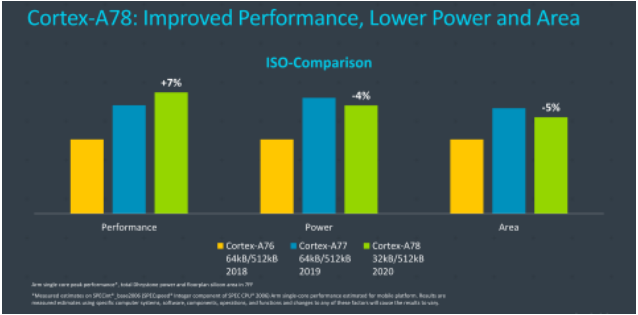
2020 year ,ARM Updated code Hercules Of A78 New architecture , It's also ARMv8 The last generation of central core architecture in the system .ARM Propagandizing this generation is “ Continuous performance and power consumption lead ”, You can see the performance improvement in the figure 20%, Process from 7nm Upgrade to 5nm, Note that performance improvement includes frequency 15% promote , Performance improvement of the architecture ARM I think it's in 7% about . Thanks to the process evolution to 5nm, Same performance , The power consumption can be compared with A77 Reduce 50%(2.1GHz amount to A77 Of 2.3GHz). As can be seen from the second picture ,A78 The main design goal of this generation is to improve performance by a small margin , Improve energy efficiency and reduce chip area .
2. A78 Some characteristics of microarchitecture


1、L1 cache :ARM Provides 32KB The choice of cache , Let some manufacturers who pay attention to cost and chip area choose lower data and instruction cache , The default is 64KB.
2、 Branch prediction : The bandwidth of branch prediction is relatively A77 Promoted 1 times .
3、 execution unit : Added one MUL unit , Allow one cycle 2 Multiplication of integers (A77 It's a cycle 1 individual ). Added one for Store Of AGU unit ,Store The ability to learn from 16B/cycle Upgrade to 32B/cycle.
A78 yes ARMv8 Build the last generation of products , It is mainly the optimization of previous generations of microarchitecture , a ARMv8 The goalkeeper of architecture .
5、 ... and 、 summary

A78 yes ARMv8 The last generation of architecture , Smart phones are still developing at a high speed and rapidly updating products ,ARM The architecture of the processor is also continuously iterating and updating .2020 year ,ARM The company proposed a plan to customize high-performance cores for manufacturers , And launched a larger area and stronger performance Cortex-X The core of the series .2021 year ,ARM The company launched a new ARMv9 framework , There are already A710、A715 Wait for products to take over A78 The route of the . Limited to space , In the future, I will continue to study with you X Series and ARMv9 Related contents of Architecture .
Abstract
1、DSU Introduce https://www.androidauthority.com/arm-dynamiq-need-to-know-770349/
2、A76 wikichip https://en.wikichip.org/wiki/arm_holdings/microarchitectures/cortex-a76
3、A77 wikichip https://en.wikichip.org/wiki/arm_holdings/microarchitectures/cortex-a77
4、A77 Introduce https://www.anandtech.com/show/14384/arm-announces-cortexa77-cpu-ip
5、Intel's Sandy Bridge Architecture Exposed https://www.anandtech.com/show/3922/intels-sandy-bridge-architecture-exposed/2
6、AMD Zen Microarchitecture https://www.anandtech.com/show/10578/amd-zen-microarchitecture-dual-schedulers-micro-op-cache-memory-hierarchy-revealed
7、A78 Introduce https://www.anandtech.com/show/15813/arm-cortex-a78-cortex-x1-cpu-ip-diverging
8、A78 wikichip https://en.wikichip.org/wiki/arm_holdings/microarchitectures/cortex-a78
9、A78 Introduce https://fuse.wikichip.org/news/3536/arm-unveils-the-cortex-a78-when-less-is-more/
10、ARMv9 Introduce https://www.anandtech.com/show/16584/arm-announces-armv9-architecture

Long press attention
Linux Kernel black Technology | Technical articles | Selected tutorials
边栏推荐
- RISC0:Towards a Unified Compilation Framework for Zero Knowledge
- Is it safe to open an account on Alipay
- Thank Huawei for sharing the developer plan
- 中移链(基于EOS)测试环境搭建
- 大咖对话:品牌扎堆数藏赛道,下半场的机遇、挑战在哪里?
- ACL 2022 | 基于最优传输的对比学习实现可解释的语义文本相似性
- 第二十周作业
- Mathematical derivation in [pumpkin Book ml] (task4) neural network
- Apipost签约中国电信!携手加速企业数字化变革
- Among the database accounts in DTS, the accounts of MySQL database and mongodb database appear most. What are the specific accounts
猜你喜欢

Use of templates

Apipost签约中国电信!携手加速企业数字化变革

Composability and Recursion in snarkyJS

大咖对话:品牌扎堆数藏赛道,下半场的机遇、挑战在哪里?
![Mathematical derivation in [pumpkin Book ml] (task4) neural network](/img/11/8d0f7254c2a22d46f2407b5f773c5c.png)
Mathematical derivation in [pumpkin Book ml] (task4) neural network
![Leetcode: the shortest dice sequence impossible to get [thinking questions + grouping ideas]](/img/89/0789cd381302237a28f3f18b3bfa74.png)
Leetcode: the shortest dice sequence impossible to get [thinking questions + grouping ideas]
day10:声明式事务控制
Composability and Recursion in snarkyJS
leetcode:不可能得到的最短骰子序列【思维题 + 分组思想】
RISC0:Towards a Unified Compilation Framework for Zero Knowledge
随机推荐
Microcomputer principle: detailed explanation of CPU architecture
Wechat applet monitoring real-time geographical location change event interface application
Metauniverse: technological evolution, industrial ecology and big country game
2022牛客多校7.23
[e-commerce operation] teach you these tips to bid farewell to invalid preset replies
Makefile基础知识--扩展
基于深度学习的多任务人脸属性分析(基于飞桨PaddlePaddle)
从A76到A78——在变化中学习ARM微架构
Ue5 reports an error using the plug-in quixel Bridge
CAD break command
Both Chen Chunhua and Mo Yan have words of suffering
Esp32485 air temperature and humidity test
Machine learning kmeans
腾讯+360+搜狗校招笔试题+知识点总结
@typescript-eslint/ [email protected]
CAD text styles
RISC0:Towards a Unified Compilation Framework for Zero Knowledge
[CCNA experiment sharing] routing between VLANs of layer 3 switches
OSI的体系结构,以及各层协议
陈春花与莫言,都有苦难言