当前位置:网站首页>Principle and Simulation of switching power supply buck circuit
Principle and Simulation of switching power supply buck circuit
2022-06-28 03:50:00 【Jiangnan small workshop】
Buck Circuit principle and simulation
The circuit principle diagram

- Buck circuit , Also known as step-down circuit , The characteristic is that the output voltage is lower than the input voltage . The input current is pulsating , The output current is continuous .
How it works
- When the switch tube Q1 The drive is high , The switch tube is on , Energy storage inductance L1 Magnetized , The current flowing through the inductor increases linearly , At the same time C1 Charge , Give load R1 Provide energy . The equivalent circuit is as follows :

- When the switch tube Q1 The drive is at low level , Switch off , Energy storage inductance L1 Discharge through freewheeling diode , Linear reduction of inductive current , The output voltage depends on the output filter capacitor C1 Discharge and reduced inductive current maintenance , The equivalent circuit is as follows :

Three working modes
CCM Mode

- Switch tube Q1 Conduction , according to KVL: V i n − L d i L d t − V o = 0 , namely L △ i L △ t = V i n − V o → L ∗ △ i L = ( V i n − V o ) ∗ △ t V_{in}-L\frac{di_{L}}{dt}-V_o=0, namely L\frac{△i_L}{△t}=V_{in}-V_o \rightarrow L*△i_L=(V_{in}-V_o)*△t Vin−LdtdiL−Vo=0, namely L△t△iL=Vin−Vo→L∗△iL=(Vin−Vo)∗△t
- △ t △t △t by Q1 On time of , △ t = T ∗ D △t=T*D △t=T∗D, T T T For duty cycle , D D D Is the duty cycle : L △ i L = ( V i n − V o ) T D L△i_L=(V_{in}-V_o)TD L△iL=(Vin−Vo)TD
- Switch tube Q1 Turn off , according to KVL( Ignore the on voltage drop of the diode ): L d i L d t = V o namely L ∗ △ i L = V o ∗ T ( 1 − D ) L\frac{di_L}{dt}=V_o namely L*△i_L=V_o*T(1-D) LdtdiL=Vo namely L∗△iL=Vo∗T(1−D)
- According to volt second balance : L △ i L = ( V i n − V o ) ∗ T ∗ D = V o ∗ T ( 1 − D ) L△i_L=(V_{in}-V_o)*T*D=V_o*T(1-D) L△iL=(Vin−Vo)∗T∗D=Vo∗T(1−D)
- Available : V o = V i n ∗ D V_o=V_{in}*D Vo=Vin∗D
- Usually when we design circuits , Often know the input and output voltage , So that we can go through D = V o V i n D=\frac{V_o}{V_{in}} D=VinVo To make sure CCM Duty cycle in mode .
- Load current Io Relationship with inductive current
- Analyze in one cycle , The load current is the average value of the current in a cycle .
- The mathematical expression of the average value of the current : I A V = ∫ 0 T i ( t ) d t T I_{AV}=\frac{\int_{0}^{T}i(t)dt}{T} IAV=T∫0Ti(t)dt
- That is, the area enclosed by the current function curve and time axis in a period divided by the period , Is the average value of the current .
- According to the previous inductance current waveform , It is known that the area in a cycle is : S = I L m i n + I L m a x 2 T ∗ D + I L m i n + I L m a x 2 T ∗ ( 1 − D ) = I L m i n + I L m a x 2 T S=\frac{I_{Lmin}+I_{Lmax}}{2}T*D+\frac{I_{Lmin}+I_{Lmax}}{2}T*(1-D)=\frac{I_{Lmin}+I_{Lmax}}{2}T S=2ILmin+ILmaxT∗D+2ILmin+ILmaxT∗(1−D)=2ILmin+ILmaxT
- therefore , The average current is I o = S T = I L m i n + I L m a x 2 I_o=\frac{S}{T}=\frac{I_{Lmin}+I_{Lmax}}{2} Io=TS=2ILmin+ILmax
BCM Mode

- contrast BCM Follow CCM The difference between : It can be found that the minimum current of the inductance gradually decreases to 0, The working mode has gradually changed from CCM Gradient to BCM. According to volt second balance : ( V i n − V o ) ∗ T ∗ D = V o ∗ T ( 1 − D ) (V_{in}-V_o)*T*D=V_o*T(1-D) (Vin−Vo)∗T∗D=Vo∗T(1−D) V o = V i n ∗ D V_o=V_{in}*D Vo=Vin∗D
- Again , Analyze in one cycle , Output average current I o I_o Io: I o = T ∗ I L m a x / 2 T = I L m a x 2 I_o=\frac{T*I_{Lmax}/2}{T}=\frac{I_{Lmax}}{2} Io=TT∗ILmax/2=2ILmax
DCM Mode

- The circuit works in DCM In mode , Two conditions need to be met :
- The current flowing through the inductor at the beginning of magnetization and the end of degaussing is zero ;
- The degaussing time of the inductor is less than the switch off time ;
- According to volt second balance : ( V i n − V o ) ∗ T ∗ D = V o ∗ T d (V_{in}-V_o)*T*D=V_o*T_d (Vin−Vo)∗T∗D=Vo∗Td V o = V i n ∗ T o n T o n + T d V_o=V_{in}*\frac{T_{on}}{T_{on}+T_d} Vo=Vin∗Ton+TdTon
- Again , Analyze in one cycle , Output average current I o I_o Io: I o = I L m a x ( T ∗ D + T d ) 2 T I_o=\frac{I_{Lmax}(T*D+T_d)}{2T} Io=2TILmax(T∗D+Td)
The relationship between inductance value and working mode
- Give a picture

- Analyze the inductive current in one cycle : I o = ( I L m i n + I L m a x ) ∗ D ∗ T 2 T + ( I L m i n + I L m a x ) ∗ T d 2 T I_o=\frac{(I_{Lmin}+I_{Lmax})*D*T}{2T}+\frac{(I_{Lmin}+I_{Lmax})*T_d}{2T} Io=2T(ILmin+ILmax)∗D∗T+2T(ILmin+ILmax)∗Td
- namely 2 T I o = ( I L m i n + I L m a x ) ∗ ( D ∗ T + T d ) 2TI_{o}=(I_{Lmin}+I_{Lmax})*(D*T+T_d) 2TIo=(ILmin+ILmax)∗(D∗T+Td)
- When Q The pipe is open : L d i L d t = V i n − V o → L I L m a x − I L m i n T D = V i n − V o L\frac{di_L}{dt}=V_{in}-V_o\rightarrow L\frac{I_{Lmax}-I_{Lmin}}{TD}=V_{in}-V_{o} LdtdiL=Vin−Vo→LTDILmax−ILmin=Vin−Vo
- namely I L m a x = ( V i n − V o ) ∗ T ∗ D L + I L m i n I_{Lmax}=\frac{(V_{in}-V_o)*T*D}{L}+I_{Lmin} ILmax=L(Vin−Vo)∗T∗D+ILmin
- Into the above equation : 2 T I o = [ I L m i n + ( V i n − V o ) T D L + I L m i n ] ( T D + T d ) 2TI_o=\left [ I_{Lmin}+\frac{(V_{in}-V_o)TD}{L}+I_{Lmin} \right ](TD+T_d) 2TIo=[ILmin+L(Vin−Vo)TD+ILmin](TD+Td) T d = 2 T L I o − 2 T D L I L m i n − V i n T 2 D 2 + V o T 2 D 2 2 L I L m i n + V i n T D − V o T D T_d=\frac{2TLI_o-2TDLI_{Lmin}-V_{in}T^2D^2+V_oT^2D^2}{2LI_{Lmin}+V_{in}TD-V_oTD} Td=2LILmin+VinTD−VoTD2TLIo−2TDLILmin−VinT2D2+VoT2D2
- If you work in DCM Pattern , Then order I L m i n = 0 , T d < T ( 1 − D ) I_{Lmin}=0,T_d<T(1-D) ILmin=0,Td<T(1−D), namely 2 T L I o − V i n T 2 D 2 + V o T 2 D 2 V i n T D − V o T D < T ( 1 − D ) → L < ( V i n − V o ) T D 2 I o \frac{2TLI_o-V_{in}T^2D^2+V_oT^2D^2}{V_{in}TD-V_oTD}<T(1-D)\rightarrow L<\frac{(V_{in}-V_o)TD}{2I_o} VinTD−VoTD2TLIo−VinT2D2+VoT2D2<T(1−D)→L<2Io(Vin−Vo)TD
- If you work in BCM Pattern , Then order I L m i n = 0 , T d = T ( 1 − D ) I_{Lmin}=0,T_d=T(1-D) ILmin=0,Td=T(1−D), namely 2 T L I o − V i n T 2 D 2 + V o T 2 D 2 V i n T D − V o T D = T ( 1 − D ) → L = ( V i n − V o ) T D 2 I o \frac{2TLI_o-V_{in}T^2D^2+V_oT^2D^2}{V_{in}TD-V_oTD}=T(1-D)\rightarrow L=\frac{(V_{in}-V_o)TD}{2I_o} VinTD−VoTD2TLIo−VinT2D2+VoT2D2=T(1−D)→L=2Io(Vin−Vo)TD
- If you work in CCM Pattern , Then order I L m i n > 0 , T d = T ( 1 − D ) I_{Lmin}>0,T_d=T(1-D) ILmin>0,Td=T(1−D), namely I L m i n = T I o T D + T d − ( V i n − V o ) T D 2 L > 0 → L > ( V i n − V o ) T D 2 I o I_{Lmin}=\frac{TI_o}{TD+T_d}-\frac{(V_{in}-V_o)TD}{2L}>0\rightarrow L>\frac{(V_{in}-V_o)TD}{2I_o} ILmin=TD+TdTIo−2L(Vin−Vo)TD>0→L>2Io(Vin−Vo)TD
Ideal design example
- Set the input voltage Ui=20V, Output voltage Uo=10V, Ripple voltage <1%,Io=1A, Switch frequency fs=100k, Try to design work in BCM The circuit of the mode meets the requirements .
- The calculation is as follows :
- Duty cycle : D = U o U i = 10 20 = 0.5 D=\frac{U_o}{U_i}=\frac{10}{20}=0.5 D=UiUo=2010=0.5
- Critical inductance of operating mode : L c = ( V i n − V o ) T D 2 I o = ( 20 − 10 ) ∗ 0.5 2 ∗ 100 k ∗ 1 = 25 u H L_c=\frac{(V_{in}-V_{o})TD}{2I_o}=\frac{(20-10)*0.5}{2*100k*1}=25uH Lc=2Io(Vin−Vo)TD=2∗100k∗1(20−10)∗0.5=25uH
- Load resistance : R L = V o I o = 10 1 = 10 Ω R_L=\frac{V_o}{I_o}=\frac{10}{1}=10Ω RL=IoVo=110=10Ω
- Output capacitance ( Don't consider ESR And transient overshoot voltage ) Calculation : C o = 1 8 f s ∗ △ i △ u = 1 8 ∗ f s ∗ I L m a x − I L m i n △ u = 1 8 ∗ 100 k ∗ 2 − 0 10 ∗ 0.01 = 25 u F C_o=\frac{1}{8f_s}*\frac{△i}{△u}=\frac{1}{8*f_s}*\frac{I_{Lmax}-I_{Lmin}}{△u}=\frac{1}{8*100k}*\frac{2-0}{10*0.01}=25uF Co=8fs1∗△u△i=8∗fs1∗△uILmax−ILmin=8∗100k1∗10∗0.012−0=25uF
saber Circuit simulation
Simulation circuit diagram

Several key device settings
Analog switch tube : stay saber Select... From the search results switch,analog SPST w/logic Enbl, Double click Add to schematic .
Set parameters
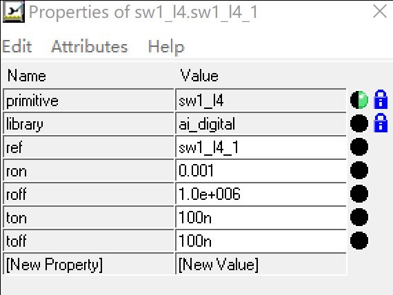
- ron: Impedance when the switch is on , It can be set as the default value 0.001;
- roff: Impedance when the switch is closed , It can be set as the default value 1M;
- ton: Switch on time ;
- toff: Switch off time ;
Driving signal
- After setting the switch tube , You need to give it a drive signal

- freq: Drive signal frequency , Set here as 100k;
- duty: Duty cycle , Set to 0.5;
- After setting the switch tube , You need to give it a drive signal
Other periods can be set by referring to the previously calculated values .
Simulation settings


Waveform analysis

- When the circuit starts simulation , The initial state of inductance and capacitance is 0, Go through an oscillating process , Reach a balance .
- Amplify the inductance current waveform , It can be seen that it works in BCM Pattern , Conform to the design .

- Amplify the output voltage , It can be seen that the ripple voltage meets the design requirements .

Closed loop control
- Compare with the above , We can find out , In open loop buck In circuit , The output voltage does not strictly follow the product of the input voltage duty cycle .
- In the actual circuit , The input power supply and output load fluctuate to some extent , The settings will change dramatically , These factors make the open-loop system unable to guarantee stable output , Therefore, feedback should be added to form a closed loop .

- Closed loop control method , At present, single closed-loop control is widely used , Most of them are closed-loop control schemes with negative voltage feedback , This is a linear control method , Simple control , The control algorithm adopts the classic PID control . By differential amplifier ,PI Regulator , as well as PWM Control composition .
Error amplifier ( Subtracter )
- The negative phase input terminal is connected to the output voltage fed back , Positive phase input termination bandgap reference voltage .
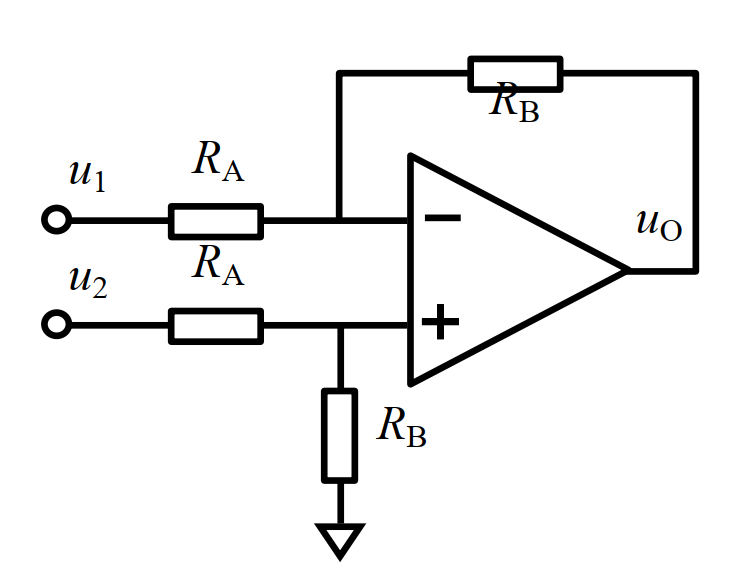
- Relation derivation : U + = R B R A + R B u 2 = U − U_{+}=\frac{R_B}{R_A+R_B}u_2=U_{-} U+=RA+RBRBu2=U− i = u 1 − U − R A = U − − u o R B i=\frac{u_1-U_{-}}{R_A}=\frac{U_{-}-u_o}{R_B} i=RAu1−U−=RBU−−uo
- Jointly available : u o = R B R A ( u 2 − u 1 ) u_o=\frac{R_B}{R_A}(u_2-u_1) uo=RARB(u2−u1)
- Draw a simulation image , And set the magnification 250, The error signal to be collected is amplified 250 times .

integrator
- Integrator regulation : The steady-state error is eliminated , Improve the accuracy . Because there are errors , Integral adjustment is done , Until there is no difference , Integral adjustment stop , The integrator outputs a constant . The strength of the integrator depends on the integration time constant σ,σ The smaller it is , The stronger the integral effect .σ The bigger it is , The weaker the integral , The dynamic response becomes slower when the integrator is added .
- Proportional regulation : To react proportionally to the deviation of a system , There is a deviation in the system , The proportional adjustment immediately produces a regulating effect to reduce the deviation . It's a big proportion , It can speed up the adjustment , But too much of it , Reduce the stability of the system .

PWM Signal generator

- The comparator is DC/DC One of the common core modules in the converter , stay DC/DC The converter can not only be used as a separate module , It can also be used as a sub circuit of other modules . Do voltage comparator application , One end is connected to the signal of the error amplifier , The other end is connected to the sawtooth wave generated by the oscillator , The two are compared to produce a pulse width modulated signal , adopt PWM The signal controls the conduction and closing of the power switch tube .
- May refer to The principle of comparator
Improved complete circuit

- Simulation run , Get the following series of waveforms

- Output voltage waveform expansion , It can be seen that under the same electrolysis , The voltage ripple is greatly reduced , And basically close to 10V Output .

边栏推荐
猜你喜欢


随机推荐
kubernetes资源对象介绍及常用命令
INFO:&nbsp; HHH000397:&nbsp; Using…
数据库系列之MySQL中的执行计划
Li Kou daily question - day 29 -219 Duplicate Element II exists
Database migration
电学基础知识整理(一)
Analysis of slow logs in MySQL and tidb of database Series
解析STEAM教育框架下未来教师研究能力
可扩展系统的“9不”原则和“5个”衡量维度
资源管理、高可用与自动化(下)
nn. Parameter and torch nn. Init series of functions to initialize model parameters
Circular sliding auto adsorption UI tool that monkeys can use
Cannot edit in read-only editor if it appears in vscode
友链须知
继承
MySQL错误
Lamaba表达式学习及常用函数式接口
How to modify a se38 editor theme
一文告诉你什么是 Kubernetes
力扣每日一题-第29天-523.在区间范围统计奇数数目