当前位置:网站首页>《牛客刷verilog》Part I Verilog快速入门
《牛客刷verilog》Part I Verilog快速入门
2022-06-25 04:00:00 【杰之行】
前言
- 之前刷过HDLbits上面的题目,点击链接可以查看详细笔记:verilog练习:hdlbits网站系列完结!
- 最近又想刷一下牛客上面的题目,可以点击链接与小编一起刷题:牛客刷题
- 小编不才,文中如有不当之处,可以在评论中互相交流。此处题目推荐看牛客的评论区,再提一嘴,注意积累自己的基本功
算法、设计模式、软件等
Part I Verilog快速入门
01. 基础语法
VL1 四选一多路器

答案
- 一个注意点: 自测运行时需要自己写testbench。第一次运行的时候,点击了自测运行。出现下面的报错,以为是自己写错了,原来是因为自测运行需要自己补充完整testbench

`timescale 1ns/1ns
module mux4_1(
input [1:0]d1,d2,d3,d0,
input [1:0]sel,
output[1:0]mux_out
);
//*************code***********//
    reg [1:0] mux_out_reg;
    [email protected](*)begin
        case(sel)
            2'd0:mux_out_reg = d3;
            2'd1:mux_out_reg = d2;
            2'd2:mux_out_reg = d1;
// 2'd3:mux_out_reg = d0;
            default:mux_out_reg = d0;
        endcase
    end
    assign mux_out = mux_out_reg;
//*************code***********//
endmodule
复盘:
- 选择器最优先想到的就是
case实现,其实这个题目也可以发散思维:如何利用二选一选择器实现四选一?
当sel为11, 输出mux_out为 d0
当sel为10, 输出mux_out为 d1
当sel为01 , 输出mux_out为 d2
当sel为00 , 输出mux_out为 d3
//伪代码表示
if (sel[1] == 1) {

	mux_out = sel[0] ? d0:d1;
} else {

	mux_out = sel[0] ? d2:d3;
}
- 此时核心代码可以表示为
//*************code***********//
    reg [1:0] mux_out_reg;
    [email protected](*)
        if (sel[1] == 1)
           mux_out_reg = sel[0] ? d0:d1;
        else
           mux_out_reg = sel[0] ? d2:d3;

    assign mux_out = mux_out_reg;
//*************code***********//
- 如果将上述always模块直接去掉,能实现吗?就是把逻辑用两个三目运算符实现了,不推荐。但小编还是想实现一下(因为它只需要一行逻辑):
//*************code***********//
    assign mux_out = (sel[1] == 1)?(sel[0] ? d0:d1):(sel[0] ? d2:d3);
//*************code***********//
VL2 异步复位的串联T触发器

答案
`timescale 1ns/1ns
module Tff_2 (
input wire data, clk, rst,
output reg q
);
//*************code***********//
    reg tmp;
    [email protected](posedge clk or negedge rst)begin
        if (!rst)
            tmp <= 1'd0;
        else if (data)
            tmp <= ~tmp;
        else
            tmp <= tmp;
    end

    [email protected](posedge clk or negedge rst)begin
        if (!rst)
            q <= 1'd0;
        else if (tmp)
            q <= ~q;
        else
            q <= q;
    end
//*************code***********//
endmodule

分析

- 从上面这张图可以得出:T 触发器的核心要点,来 1 翻转,来 0 保持。
- 根据原理,就很容易得到上面的答案。但是,注意观察真值表,还会得到逻辑表达式:
Q* = T ^ Q,于是可以将核心代码简化:
//*************code***********//
    reg tmp;
    [email protected](posedge clk or negedge rst)begin
        if (!rst)
            tmp <= 1'd0;
        else
            tmp <= data ^ tmp;
    end

    [email protected](posedge clk or negedge rst)begin
        if (!rst)
            q <= 1'd0;
        else
            q <= tmp ^ q;
    end
//*************code***********//
- 注意思考,T 触发器的核心要点,来 1 翻转,来 0 保持。可以不可以理解为,门控时钟的一种体现?
复盘
注意 T 触发器:来 1 翻转,来 0 保持。
注意理解同步复位和异步复位。
异步复位的缺点:产生毛刺(容易造成亚稳态)
同步复位的缺点:同步复位的电路实现,比异步复位的电路实现,要浪费更多电路资源
关于浪费资源这一点,由于很多fpga自带异步复位,所以同步复位会多增加一个mux

那么结合两者,避免产生亚稳态的同时也充分利用资源,可以采用异步复位同步释放。
常用的异步复位同步释放图:

这里博客中给出了一系列经常容易迷惑的点的解答
1.直接接入异步复位信号驱动复位端有啥问题?
就是常说的异步复位产生亚稳态
2.两级触发器同步,就能消除亚稳态吗?
不能,但能大大减少
3.如果只做一级触发器同步,如何?
不可以。第一级触发器的输出,永远存在亚稳态的可能。亚稳态,导致系统不会复位初始化到已知状态。
当第一级触发器采样异步输入之后,允许输出出现的亚稳态可以长达一个周期,在这个周期内,亚稳态特性减弱。在第二个时钟沿到来时,第二级同步器采样,之后才把该信号传递到内部逻辑中去。第二级输出是稳定且已被同步了的。如果在第二级采样时保持时间不够,第一级的输出仍然处于很强的亚稳态,将会导致第二级同步器也进入亚稳态,但这种故障出现的概率比较小。
4.复位同步器,第2个dff是否存在亚稳态?(这个最让人迷惑)
只有当DFF的数据输入端口和数据输出端口,存在值不同的情况下,才会有recovery timing/removal timing问题。
第1个dff的数据输入端口和数据输出端口,在异步复位释放的时刻,是1和0,所以会有竞争冒险,有概率产生亚稳态;
第2个dff的数据输入端口和数据输出端口,在异步复位释放的时刻,是0和0,所以不存在竞争冒险,不会产生亚稳态。
因为第1个dff有概率产生亚稳态,为了防止传播,所以,多加几级dff,降低亚稳态的传播概率是有益处的。
上面九成问题的答案都转自博客,需要强调的是,现代数字芯片设计,强调的都是同步复位,这样有利于STA(静态时序分析),便于移植。
RTL原理图如下:
这里Q和D连接我认为可能是逻辑表达式要求和当前状态有关,但说实话,我不清楚这两个模块RTL内部的结构,无法做进一步分析。
测试代码如下:

主要就是clk和data数据的编写
得到的仿真波形如下:

当data为1的时刻,时钟一旦采样到,下一个时钟上升沿则中间输出翻转,而中间输出每两个时钟周期产生一次持续一个周期的高电平,这带来最终输入翻转,每次翻转应该为两个周期一次。且滞后一个周期。
当data为0的时候,若中间输出为一,最终输出继续翻转,若为零,保持不变(波形仅仅涵盖第二种结果。
VL3 奇偶校验

答案
`timescale 1ns/1ns
module odd_sel(
input [31:0] bus,
input sel,
output check
);
//*************code***********//

    assign check = sel ? (^bus) : ~(^bus);

//*************code***********//
endmodule

分析
1、奇偶校验,通过校验位使得1的个数恰好是奇数个或偶数个
奇校验:原始码流+校验位 总共有奇数个1
偶校验:原始码流+校验位 总共有偶数个1
说人话,
对于奇校验,如果原始码流中1的个数是偶数个,那么校验位就是1, 否则就是0;
对于奇校验,如果原始码流中1的个数是奇数个,那么校验位就是0, 否则就是1;
对于偶校验,如果原始码流中1的个数是偶数个,那么校验位就是0, 否则就是1;
对于偶校验,如果原始码流中1的个数是奇数个,那么校验位就是1, 否则就是0;
2、判断原始码流中的1的个数是偶数个还是奇数个
- 此处很容易想到异或操作,
0011_1111_1111_1111按位异或得到的值是1,此时的1就是奇校验位;如果求偶校验位,取反即可
3、写出伪代码如下:
if (sel == 1)//求奇校验
	check = ^bus;
else
	check = ~(^bus);
- 此时很容易想到三目运算符写答案:
assign check = sel ? (^bus) : ~(^bus);
复盘
- 此处注意思考,
单目运算符和缩减运算符。需要对其一个概念,缩减运算符是单目运算符,但是单目运算符不一定是缩减运算符。

VL4 移位运算与乘法
答案
`timescale 1ns/1ns
module multi_sel(
input [7:0]d ,
input clk,
input rst,
output reg input_grant,
output reg [10:0]out
);
//*************code***********//
    reg[1:0] cnt_4;
    [email protected](posedge clk or negedge rst)begin
        if(!rst)
            cnt_4 <= 'd0;
        else if(cnt_4 == 2'b11)
            cnt_4 <= 'd0;
        else cnt_4 <= cnt_4 + 1'b1;
    end

    reg [7:0] d_reg;
    [email protected](posedge clk or negedge rst)begin
        if(!rst)begin
                input_grant <= 'b0;
                out <= 'd0;
        end
        else if(cnt_4 == 'd0)begin
                input_grant <= 'b1;
                d_reg <= d;
                out <= d;
        end
        else if(cnt_4 == 'd1)begin
                input_grant <= 'b0;
                out <= d_reg * 3;
        end

         else if(cnt_4 == 'd2)begin
                input_grant <= 'b0;
                out <= d_reg * 7;
        end

            else if(cnt_4 == 'd3)begin
                input_grant <= 'b0;
                out <= d_reg * 8;
        end
    end
//*************code***********//
endmodule
复盘
- 题目中明确给出了四拍处理一个输入,很常见的就是设置一个计数器,用两位的计数器就可以统计四个状态,
也不用自己计数清零了。 - 上述的使用了带有优先级的
if -else结构,可以优化为case结构,小编就不改写这部分了,下一题用到了case结构。 - 上面的信号可以单独分开书写,优化效果如下:
//*************code***********//
    reg[1:0] cnt_4;
    [email protected](posedge clk or negedge rst)begin
        if(!rst)
            cnt_4 <= 'd0;
        else
            cnt_4 <= cnt_4 + 1'b1;
    end

    reg [7:0] d_reg;
    [email protected](posedge clk or negedge rst)begin
        if(!rst)begin
            input_grant <= 'b0;
            out <= 'd0;
        end
        else if(cnt_4 == 'd0)begin
            d_reg <= d;
            out <= d;
        end
        else if(cnt_4 == 'd1)begin
            out <= d_reg * 3;
        end
         else if(cnt_4 == 'd2)begin
            out <= d_reg * 7;
        end
        else if(cnt_4 == 'd3)begin
            out <= d_reg * 8;
        end
    end

    [email protected](posedge clk or negedge rst)begin
        if(!rst)begin
            input_grant <= 'b0;
        end
        else if(cnt_4 == 'd0)begin
            input_grant <= 'b1;
        end
        else begin
            input_grant <= 'b0;
        end
    end
//*************code***********//
VL5 位拆分与运算

答案
`timescale 1ns/1ns

module data_cal(
input clk,
input rst,
input [15:0]d,
input [1:0]sel,

output [4:0]out,
output validout
);
//*************code***********//
    reg validout;
    always @ (posedge clk or negedge rst)begin
        if (!rst)begin
            validout <= 1'b0;
        end
        else if (sel == 2'b0) begin
            validout <= 1'b0;
        end  else begin
            validout <= 1'b1;
        end
    end

    reg [15:0] d_reg;
    always @ (posedge clk or negedge rst)begin
        if (!rst)begin
            d_reg <= 'd0;
        end
        else if (sel == 0)begin
            d_reg <= d;
        end
// else begin
// d_reg <= d_reg;
// end
    end

    reg [4:0]out;
    always @ (posedge clk or negedge rst)begin
        if (!rst)begin
            out <= 'd0;
        end
        else case(sel)
            2'b00:out <= 'd0;
            2'b01:out <= d_reg[3:0] + d_reg[7:4];
            2'b10:out <= d_reg[3:0] + d_reg[11:8];
            2'b11:out <= d_reg[3:0] + d_reg[15:12];
        endcase
    end
//*************code***********//
endmodule

复盘
- 注意思考
d_reg的作用,这个信号究竟起着什么作用,还有注释掉的三行代码在工程实践中是否可以完全省略? case 结构怎么与if-else结构互换?
VL6 多功能数据处理器

答案
`timescale 1ns/1ns
module data_select(
	input clk,
	input rst_n,
	input signed[7:0]a,
	input signed[7:0]b,
	input [1:0]select,
	output reg signed [8:0]c
);

    [email protected](posedge clk or negedge rst_n)begin
        if (!rst_n)
            c <= 'd0;
        else case(select)
            2'b00:c <= a;
            2'b01:c <= b;
            2'b10:c <= a+b;
            2'b11:c <= a-b;
        endcase
    end
endmodule

复盘
- 有没有觉得和上面几道题思路完全一致
VL7 求两个数的差值

答案
`timescale 1ns/1ns
module data_minus(
	input clk,
	input rst_n,
	input [7:0]a,
	input [7:0]b,

	output  reg [8:0]c
);
    [email protected](posedge clk or negedge rst_n)
    if (!rst_n)
            c <= 'd0;
    else
        c <= (a > b) ? (a - b) : (b-a);
endmodule

VL8 使用generate…for语句简化代码

答案
`timescale 1ns/1ns
module gen_for_module(
    input [7:0] data_in,
    output [7:0] data_out
);
    genvar i;
    generate for( i = 0; i < 8; i = i + 1 )
// begin:generate_1
            assign data_out [i] = data_in [7 - i];
// end
    endgenerate

endmodule

复盘
- 下面是别人写的笔记,请看小编上面的答案,还故意把第2条信息给违背了?
WHY?想必你可以自行判断正误


- 还有注意第一条为什么需要满足?个人觉得可以结合
动态变量进行理解!
VL9 使用子模块实现三输入数的大小比较

答案
`timescale 1ns/1ns
module main_mod(
	input clk,
	input rst_n,
	input [7:0]a,
	input [7:0]b,
	input [7:0]c,

	output [7:0]d
);

    wire [7:0] min1, min2;

   min_mod min1_mod(
       .clk(clk),
       .rst_n(rst_n),
       .a(a),
       .b(b),
       .min(min1)
   );

    min_mod min2_mod(
        .clk(clk),
        .rst_n(rst_n),
        .a(a),
        .b(c),
        .min(min2)
   );

    min_mod min3_mod(
        .clk(clk),
        .rst_n(rst_n),
        .a(min1),
        .b(min2),
        .min(d)
   );
// assign d = min1 > min2 ? min2 : min1;
endmodule


module min_mod(
	input clk,
	input rst_n,
	input [7:0]a,
	input [7:0]b,

    output reg [7:0]min
);
    [email protected](posedge clk or negedge rst_n)
        if(!rst_n)
            min <= 'd0;
        else
            min <= (a > b) ? b : a;

endmodule

复盘
- 题目中要求使用子模块进行大小比较
- 注意时序要求:本想着节约一拍的时间,就写成了如下的形式,给报错了。
`timescale 1ns/1ns
module main_mod(
	input clk,
	input rst_n,
	input [7:0]a,
	input [7:0]b,
	input [7:0]c,

	output [7:0]d
);

    wire [7:0] min1, min2;

   min_mod min1_mod(
       .clk(clk),
       .rst_n(rst_n),
       .a(a),
       .b(b),
       .min(min1)
   );

    min_mod min2_mod(
        .clk(clk),
        .rst_n(rst_n),
        .a(a),
        .b(c),
        .min(min2)
   );

// min_mod min3_mod(
// .clk(clk),
// .rst_n(rst_n),
// .a(min1),
// .b(min2),
// .min(d)
// );

    assign d = min1 > min2 ? min2 : min1;

endmodule


module min_mod(
	input clk,
	input rst_n,
	input [7:0]a,
	input [7:0]b,

    output reg [7:0]min
);
    [email protected](posedge clk or negedge rst_n)
        if(!rst_n)
            min <= 'd0;
        else
            min <= (a > b) ? b : a;

endmodule

VL10 使用函数实现数据大小端转换

答案
`timescale 1ns/1ns
module function_mod(
    input clk,
    input rst_n,
	input [3:0]a,
	input [3:0]b,

	output [3:0]c,
	output [3:0]d
);

    function [3:0] reverse;
        input [3:0] data_in;
        begin
            reverse[0] = data_in[3];
            reverse[1] = data_in[2];
            reverse[2] = data_in[1];
            reverse[3] = data_in[0];
        end
    endfunction

    assign c = reverse(a);
    assign d = reverse(b);
endmodule

复盘
- 不想过多的解释,题目中原始端口竟然没有
clk和rst_n,而且题目中还说,c和d都是8bit的。。。 - 大小端,是针对字节序而言的。此题可以说是比特位反转,再说,这一功能用
流操作一行代码就可以搞定,设计人员赶快学学systemverilog。
02. 组合逻辑
VL11 4位数值比较器电路

答案
`timescale 1ns/1ns

module comparator_4(
	input		[3:0]       A   	,
	input	   [3:0]		B   	,

 	output	 reg		Y2    , //A>B
	output   reg        Y1    , //A=B
    output   reg        Y0      //A<B
);

    [email protected](*)begin
        if (A[3] > B[3])
            {
    Y2,Y1,Y0} = 3'b100;
        else if (A[3] < B[3])
            {
    Y2,Y1,Y0} = 3'b001;
        else if (A[2] > B[2])
            {
    Y2,Y1,Y0} = 3'b100;
        else if (A[2] < B[2])
            {
    Y2,Y1,Y0} = 3'b001;

        else if (A[1] > B[1])
            {
    Y2,Y1,Y0} = 3'b100;
        else if (A[1] < B[1])
            {
    Y2,Y1,Y0} = 3'b001;
        else if (A[0] > B[0])
            {
    Y2,Y1,Y0} = 3'b100;
        else if (A[0] < B[0])
            {
    Y2,Y1,Y0} = 3'b001;
        else
            {
    Y2,Y1,Y0} = 3'b010;
    end

endmodule

复盘
- 上面全部使用了
if-else这种结构,它存在优先级关系,个人看来也是最容易理解的一种方式。 - 在实际项目中,并不是一下子就写出很稳健的程序,后期就是不断的优化,利用各种各样先进的算法、甚至加入设计模式来优化。
- 上面题目答案,我将接口定义的输出端口由
wire类型改为了reg类型,为什么呢?(自己想,就是不想打字了) - 接下面再将输出一致的情况合并,代码如下:
`timescale 1ns/1ns

module comparator_4(
	input		[3:0]       A   	,
	input	   [3:0]		B   	,

 	output	 reg		Y2    , //A>B
	output   reg        Y1    , //A=B
    output   reg        Y0      //A<B
);

    [email protected](*)begin
        if ((A[3] > B[3]) || ((A[3] == B[3]) &&  (A[2] > B[2])) || ((A[3] == B[3]) &&  (A[2] == B[2]) &&  (A[1] > B[1])) || ((A[3] == B[3]) &&  (A[2] == B[2]) &&  (A[1] == B[1]) &&  (A[0] > B[0])))
            {
    Y2,Y1,Y0} = 3'b100;
        else if ((A[3] < B[3]) || ((A[3] == B[3]) &&  (A[2] < B[2])) || ((A[3] == B[3]) &&  (A[2] == B[2]) &&  (A[1] < B[1])) || ((A[3] == B[3]) &&  (A[2] == B[2]) &&  (A[1] == B[1]) &&  (A[0] < B[0])))
            {
    Y2,Y1,Y0} = 3'b001;
        else
            {
    Y2,Y1,Y0} = 3'b010;
    end

endmodule
- 基于上述代码,继续优化,变量默认初始值都是0,我们只需要关注什么时候产生1,于是继续优化,代码如下:
`timescale 1ns/1ns

module comparator_4(
	input		[3:0]       A   	,
	input	   [3:0]		B   	,

 	output	 reg		Y2    , //A>B
	output   reg        Y1    , //A=B
    output   reg        Y0      //A<B
);

    [email protected](*)begin
            Y2 = ((A[3] > B[3]) || ((A[3] == B[3]) &&  (A[2] > B[2])) || ((A[3] == B[3]) &&  (A[2] == B[2]) &&  (A[1] > B[1])) || ((A[3] == B[3]) &&  (A[2] == B[2]) &&  (A[1] == B[1]) &&  (A[0] > B[0]))) ? 1'b1 : 1'b0;
            Y0 = ((A[3] < B[3]) || ((A[3] == B[3]) &&  (A[2] < B[2])) || ((A[3] == B[3]) &&  (A[2] == B[2]) &&  (A[1] < B[1])) || ((A[3] == B[3]) &&  (A[2] == B[2]) &&  (A[1] == B[1]) &&  (A[0] < B[0]))) ? 1'b1 : 1'b0;
            Y1 = ((A[3] == B[3]) &&  (A[2] == B[2]) &&  (A[1] == B[1]) &&  (A[0] == B[0]))  ? 1'b1 : 1'b0;
    end

endmodule
- 继续优化,Y1的逻辑可以简写成这样
Y1 = (A == B) ? 1'b1 : 1'b0;,甚至直接写成Y1 = A == B;还有三者的变量不同时为1,所以除Y1的变量可以写成其他两个变量取反
`timescale 1ns/1ns

module comparator_4(
	input		[3:0]       A   	,
	input	   [3:0]		B   	,

 	output	 reg		Y2    , //A>B
	output   reg        Y1    , //A=B
    output   reg        Y0      //A<B
);

    [email protected](*)begin
            Y2 = (A[3] > B[3]) || ((A[3] == B[3]) &&  (A[2] > B[2])) || ((A[3] == B[3]) &&  (A[2] == B[2]) &&  (A[1] > B[1])) || ((A[3] == B[3]) &&  (A[2] == B[2]) &&  (A[1] == B[1]) &&  (A[0] > B[0]));
            Y1 = A == B;
            Y0 = ~(Y2 || Y1);
    end

endmodule
- 此时此刻, 突然想把输出端口的reg类型改为原来的wire类型,那我们需要用assign语句了,继续改造,但是报错了,小编并不觉得错了,如果发现了错误可以在评论区指出来哈。
`timescale 1ns/1ns

module comparator_4(
	input		[3:0]       A   	,
	input	   [3:0]		B   	,

 	output	 wire		Y2    , //A>B
	output   wire       Y1    , //A=B
    output   wire       Y0      //A<B
);

    assign    Y1 = A == B;
    assign    Y2 = (A[3] > B[3]) || ((A[3] == B[3]) &&  (A[2] > B[2])) || ((A[3] == B[3]) &&  (A[2] == B[2]) &&  (A[1] > B[1])) || ((A[3] == B[3]) &&  (A[2] == B[2]) &&  (A[1] == B[1]) &&  (A[0] > B[0]));
    assign    Y0 = ~(Y2 || Y1);

endmodule

VL12 4bit超前进位加法器电路

答案
`timescale 1ns/1ns

module lca_4(
	input		[3:0]       A_in  ,
	input	    [3:0]		B_in  ,
    input                   C_1   ,

 	output	 wire			CO    ,
	output   wire [3:0]	    S
);


    wire [3:0] G;
    wire [3:0] P;

    assign G[0] = A_in[0] & B_in[0];
    assign G[1] = A_in[1] & B_in[1];
    assign G[2] = A_in[2] & B_in[2];
    assign G[3] = A_in[3] & B_in[3];

    assign P[0] = A_in[0] ^ B_in[0];
    assign P[1] = A_in[1] ^ B_in[1];
    assign P[2] = A_in[2] ^ B_in[2];
    assign P[3] = A_in[3] ^ B_in[3];

    wire [3:0] C;

    assign S[0] = P[0] ^ C_1;
    assign S[1] = P[1] ^ C[0];
    assign S[2] = P[2] ^ C[1];
    assign S[3] = P[3] ^ C[2];
    assign CO = C[3];

    assign C[0] = G[0] | P[0]&C_1;
    assign C[1] = G[1] | P[1]&C[0];
    assign C[2] = G[2] | P[2]&C[1];
    assign C[3] = G[3] | P[3]&C[2];


endmodule

复盘
- 此处推荐一篇文章3-2 Verilog 4位行波进位加法器,还有可以了解一下
行波进位(Ripple Carry)与超前进位(Loodahead Carry) - 刚开始学习的时候就很迷糊,这部分就不展开胡说了。
VL13 优先编码器电路①

答案
`timescale 1ns/1ns

module encoder_0(
   input      [8:0]         I_n   ,

   output reg [3:0]         Y_n
);
    always @ (*)
      begin
        casex(I_n)
          9'b1_1111_1111 : Y_n = 4'b1111;
          9'b0_xxxx_xxxx : Y_n = 4'b0110;
          9'b1_0xxx_xxxx : Y_n = 4'b0111;
          9'b1_10xx_xxxx : Y_n = 4'b1000;
          9'b1_110x_xxxx : Y_n = 4'b1001;
          9'b1_1110_xxxx : Y_n = 4'b1010;
          9'b1_1111_0xxx : Y_n = 4'b1011;
          9'b1_1111_10xx : Y_n = 4'b1100;
          9'b1_1111_110x : Y_n = 4'b1101;
          9'b1_1111_1110 : Y_n = 4'b1110;
          default : Y_n = 4'b1111;
        endcase
      end
endmodule
复盘
- 答案已经在下一题给出了,哈哈哈
VL14 用优先编码器①实现键盘编码电路

答案
`timescale 1ns/1ns
module encoder_0(
   input      [8:0]         I_n   ,

   output reg [3:0]         Y_n
);

always @(*)begin
   casex(I_n)
      9'b111111111 : Y_n = 4'b1111;
      9'b0xxxxxxxx : Y_n = 4'b0110;
      9'b10xxxxxxx : Y_n = 4'b0111;
      9'b110xxxxxx : Y_n = 4'b1000;
      9'b1110xxxxx : Y_n = 4'b1001;
      9'b11110xxxx : Y_n = 4'b1010;
      9'b111110xxx : Y_n = 4'b1011;
      9'b1111110xx : Y_n = 4'b1100;
      9'b11111110x : Y_n = 4'b1101;
      9'b111111110 : Y_n = 4'b1110;
      default      : Y_n = 4'b1111;
   endcase
end

endmodule

module key_encoder(
      input      [9:0]         S_n   ,

      output wire[3:0]         L     ,
      output wire              GS
);

    wire   [3:0]  Y_n;
    encoder_0 encoder(
       .I_n   (S_n[9:1]),
       .Y_n   (Y_n)
    );

    assign L = ~Y_n;
// assign GS = ~(S_n[0] & Y_n[0] & Y_n[1] & Y_n[2] & Y_n[3]);
    assign GS = ((Y_n == 4'b1111) && (S_n[0] == 1)) ? 0 : 1;
endmodule

VL15 优先编码器Ⅰ

答案
`timescale 1ns/1ns

module encoder_83(
   input      [7:0]       I   ,
   input                  EI  ,

   output wire [2:0]      Y   ,
   output wire            GS  ,
   output wire            EO
);
    reg [4:0] temp;
    assign {
    Y[2:0],GS,EO} = temp;
    [email protected](*) begin
        casex({
    EI,I[7:0]})
            9'b0_xxxx_xxxx: temp = 5'b000_00;
            9'b1_0000_0000: temp = 5'b000_01;
            9'b1_1xxx_xxxx: temp = 5'b111_10;
            9'b1_01xx_xxxx: temp = 5'b110_10;
            9'b1_001x_xxxx: temp = 5'b101_10;
            9'b1_0001_xxxx: temp = 5'b100_10;
            9'b1_0000_1xxx: temp = 5'b011_10;
            9'b1_0000_01xx: temp = 5'b010_10;
            9'b1_0000_001x: temp = 5'b001_10;
            9'b1_0000_0001: temp = 5'b000_10;
        endcase
    end
endmodule

复盘
- 这种译码器最简单的实现方式就是,你把码表直接实现一遍即可。
- 比如,这部分的数字和题目中的完全一致
			9'b0_xxxx_xxxx: temp = 5'b000_00;
            9'b1_0000_0000: temp = 5'b000_01;
            9'b1_1xxx_xxxx: temp = 5'b111_10;
            9'b1_01xx_xxxx: temp = 5'b110_10;
            9'b1_001x_xxxx: temp = 5'b101_10;
            9'b1_0001_xxxx: temp = 5'b100_10;
            9'b1_0000_1xxx: temp = 5'b011_10;
            9'b1_0000_01xx: temp = 5'b010_10;
            9'b1_0000_001x: temp = 5'b001_10;
            9'b1_0000_0001: temp = 5'b000_10;
- 当然,还有其他实现方式,比如下题中给出的就是
VL16 使用8线-3线优先编码器Ⅰ实现16线-4线优先编码器

答案
`timescale 1ns/1ns
module encoder_83(
   input      [7:0]       I   ,
   input                  EI  ,

   output wire [2:0]      Y   ,
   output wire            GS  ,
   output wire            EO
);
assign Y[2] = EI & (I[7] | I[6] | I[5] | I[4]);
assign Y[1] = EI & (I[7] | I[6] | ~I[5]&~I[4]&I[3] | ~I[5]&~I[4]&I[2]);
assign Y[0] = EI & (I[7] | ~I[6]&I[5] | ~I[6]&~I[4]&I[3] | ~I[6]&~I[4]&~I[2]&I[1]);

assign EO = EI&~I[7]&~I[6]&~I[5]&~I[4]&~I[3]&~I[2]&~I[1]&~I[0];

assign GS = EI&(I[7] | I[6] | I[5] | I[4] | I[3] | I[2] | I[1] | I[0]);
//assign GS = EI&(| I);

endmodule

module encoder_164(
   input      [15:0]      A   ,
   input                  EI  ,

   output wire [3:0]      L   ,
   output wire            GS  ,
   output wire            EO
);
    wire [2:0] Y_1,Y_0;
    wire gs_1,gs_0;
    wire EO1;

    encoder_83    encoder_83_U1(
        .I  (A[15:8]),
        .EI (EI),

        .Y  (Y_1),
        .GS (gs_1),
        .EO (EO1)
    );

    encoder_83    encoder_83_U0(
        .I (A[7:0]),
        .EI (EO1),

        .Y  (Y_0),
        .GS (gs_0),
        .EO (EO)
    );
    assign L = {
    gs_1,Y_1[2]|Y_0[2],Y_1[1]|Y_0[1],Y_1[0]|Y_0[0]};
    assign GS = gs_1|gs_0;

endmodule
复盘
- 抄的,题目晦涩难懂
VL17 用3-8译码器实现全减器

答案
- 不想做,题目截图,防止后期题库更新就截图当快照了
VL18 实现3-8译码器①
中等 通过率:37.98%
描述
下表是74HC138译码器的功能表
①请用基础门电路实现该译码器电路,用Verilog将电路描述出来。基础门电路包括:非门、多输入与门、多输入或门。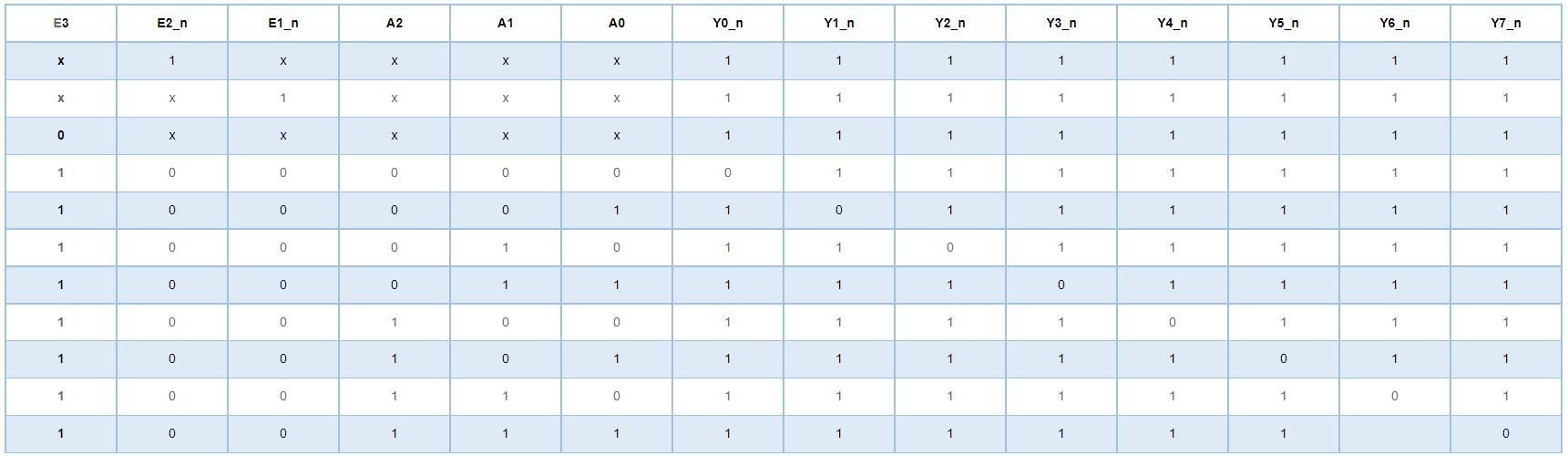
输入描述:
input E1_n ,
input E2_n ,
input E3 ,
input A0 ,
input A1 ,
input A2
输出描述:
output wire Y0_n ,
output wire Y1_n ,
output wire Y2_n ,
output wire Y3_n ,
output wire Y4_n ,
output wire Y5_n ,
output wire Y6_n ,
output wire Y7_n
答案
- 不想做,题目截图,防止后期题库更新就截图当快照了
VL19 使用3-8译码器①实现逻辑函数
- 略
VL20 数据选择器实现逻辑电路
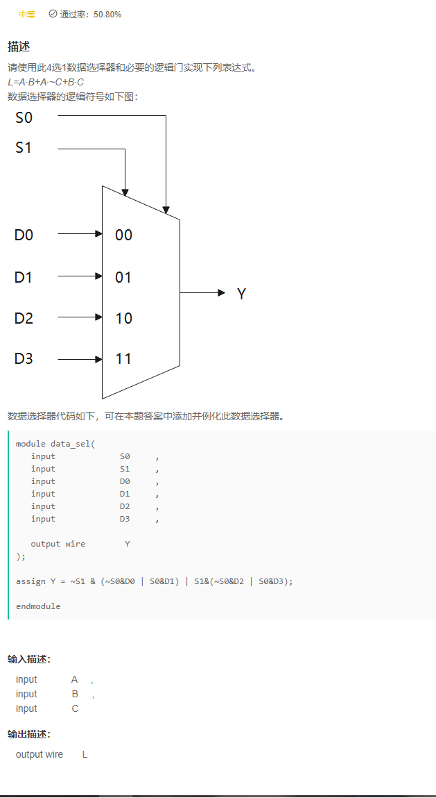
答案
`timescale 1ns/1ns

module data_sel(
   input             S0     ,
   input             S1     ,
   input             D0     ,
   input             D1     ,
   input             D2     ,
   input             D3     ,

   output wire        Y
);

assign Y = ~S1 & (~S0&D0 | S0&D1) | S1&(~S0&D2 | S0&D3);

endmodule

module sel_exp(
   input             A     ,
   input             B     ,
   input             C     ,

   output wire       L
);
    data_sel u(
        .S1('b0),
        .S0(C),

        .D1(B),
        .D0(A),
        .Y(L)
    );
endmodule
03. 时序逻辑
VL21 根据状态转移表实现时序电路
答案
`timescale 1ns/1ns

module seq_circuit(
      input                A   ,
      input                clk ,
      input                rst_n,

      output   wire        Y
);
    reg [1:0] cur_state,next_state;
    reg Y_temp;
    assign Y=Y_temp;

    parameter S0=2'b00;
    parameter S1=2'b01;
    parameter S2=2'b10;
    parameter S3=2'b11;

    [email protected](posedge clk or negedge rst_n)begin
        if(~rst_n)
            cur_state<=S0;
        else
            cur_state<=next_state;
    end

    [email protected](*)begin
        case(cur_state)
            S0:begin
                if(A==0)
                    next_state=S1;
                else
                    next_state=S3;
            end
            S1:begin
                if(A==0)
                    next_state=S2;
                else
                    next_state=S0;
            end
            S2:begin
                if(A==0)
                    next_state=S3;
                else
                    next_state=S1;
            end
            S3:begin
                if(A==0)
                    next_state=S0;
                else
                    next_state=S2;
            end
            default:next_state=S0;
        endcase
    end

    [email protected](*)begin
        if(cur_state==S3)
            Y_temp=1;
        else
            Y_temp=0;
    end

endmodule
复盘
下面这幅图能不能看懂

有了这个表再画出·状态转移图就相当于完成了

接下来尝试优化代码。
VL22 根据状态转移图实现时序电路

答案
`timescale 1ns/1ns

module seq_circuit(
   input                C   ,
   input                clk ,
   input                rst_n,

   output   wire        Y
);

    reg [1:0] cur_state,next_state;
    reg Y_temp;
    assign Y=Y_temp;

    parameter S0=2'b00;
    parameter S1=2'b01;
    parameter S2=2'b10;
    parameter S3=2'b11;

    [email protected](posedge clk or negedge rst_n)begin
        if(~rst_n)
            cur_state<=S0;
        else
            cur_state<=next_state;
    end

    [email protected](*)begin
        case(cur_state)
            S0:begin
                if(C==0)
                    next_state=S0;
                else
                    next_state=S1;
            end
            S1:begin
                if(C==0)
                    next_state=S3;
                else
                    next_state=S1;
            end
            S2:begin
                if(C==0)
                    next_state=S0;
                else
                    next_state=S2;
            end
            S3:begin
                if(C==0)
                    next_state=S3;
                else
                    next_state=S2;
            end
            default:next_state=S0;
        endcase
    end

    [email protected](*)begin
        if(cur_state==S3 || (cur_state==S2 && C == 1))
            Y_temp=1;
        else
            Y_temp=0;
    end


endmodule

复盘
- 直接修改上一题的代码就可以
VL23 ROM的简单实现

答案
`timescale 1ns/1ns
module rom(
	input clk,
	input rst_n,
	input [7:0]addr,

	output [3:0]data
);

    reg [3:0] romreg[7:0];

    always @ (posedge clk or negedge rst_n)
    begin
        if( ~rst_n ) begin
            romreg[0] <= 4'd0;
            romreg[1] <= 4'd2;
            romreg[2] <= 4'd4;
            romreg[3] <= 4'd6;
            romreg[4] <= 4'd8;
            romreg[5] <= 4'd10;
            romreg[6] <= 4'd12;
            romreg[7] <= 4'd14;
        end
// else begin
// romreg[0] <= 4'd0;
// romreg[1] <= 4'd2;
// romreg[2] <= 4'd4;
// romreg[3] <= 4'd6;
// romreg[4] <= 4'd8;
// romreg[5] <= 4'd10;
// romreg[6] <= 4'd12;
// romreg[7] <= 4'd14;
// end
    end

    assign data = romreg[addr];

endmodule

复盘
- 其实这个只读寄存器,初始化之后就不会改变了,因此只需要在
赋值的时候赋入初值即可,在实际项目中多通过读取Men配置文件来初始化。 - 有规律的初始化,肯定不会按个赋值了,找到规律,可以快速开发。优化代码如下:
`timescale 1ns/1ns
module rom(
	input clk,
	input rst_n,
	input [7:0]addr,

	output [3:0]data
);

    reg [3:0] romreg[7:0];
    integer i;
    always @ (posedge clk or negedge rst_n)
        if( ~rst_n ) begin
            for(i = 0; i < 8; i = i+1) begin : rom_i
                romreg[i] <= 2*i;
            end
        end

    assign data = romreg[addr];

endmodule
VL24 边沿检测

答案
`timescale 1ns/1ns
module edge_detect(
	input clk,
	input rst_n,
	input a,

	output reg rise,
	output reg down
);

    reg a_reg;

    [email protected](posedge clk or negedge rst_n)
        if(!rst_n)begin
            a_reg <= 1'b0;
            rise <= 1'b0;
            down <= 1'b0;
        end
        else begin
            a_reg <= a;
            if(a & ~a_reg)
                rise <= 1'b1;
            else
                rise <= 1'b0;
            if(~a & a_reg)
                down <= 1'b1;
            else
                down <= 1'b0;
        end

endmodule

复盘
- 注意审题,题目中明确说到,
下一个时钟沿就拉高,意味着,不能再使用两级寄存器打两拍。
Part II Verilog进阶挑战
Part III Verilog企业真题
后记
推荐相关文章
边栏推荐
- Numpy NP tips: squeeze and other processing of numpy arrays
- Mongodb cluster
- Data import and export for gbase 8s
- JS arrow function
- Blob page in gbase 8s
- BSC smart contract dividend mainstream currency | including marketing wallet | deflation | reflow | dividend free token | available for direct deployment
- 简单的恶意样本行文分析-入门篇
- Musk released humanoid robot. Why is AI significant to musk?
- GBASE 8s的并行操作问题场景描述
- Laravel document sorting 6. Response
猜你喜欢

Laravel document sorting 4. Controller

Unit test coverage

机器学习深度学习——向量化

GBASE 8s 索引R树
单元测试覆盖率

Finereport displays and hides column data according to conditions

Gbase 8s overall architecture

NFT insider 63: the sandbox reached a cooperation with Time magazine, and YGG established Spain's subdao

什么是存储引擎以及MySQL常见的三种数据库存储引擎

深度学习——几种学习类型
随机推荐
记录小知识点
SQL injection details
GBase 8s 锁的分类
What is persistence? What are RDB and AOF in redis persistence?
GBase 8s的封锁技术的基本介绍
Laravel document sorting 9. Blade template
Data import and export for gbase 8s
Introduction to the isolation level of gbase 8s
L'épée leetcode fait référence au chemin leetcode de l'offre II 091 pour peindre la maison [planification dynamique] heroding
Coinlist queuing tutorial to improve the winning rate
GBASE 8s中DELIMIDENT环境变量的使用
第二十五周记录
CTF_ Web: Advanced questions of attack and defense world expert zone WP (1-4)
Office macro virus bounce shell experiment
English Grammar - pronunciation rules
@Requestbody solution get parameter is null
什么是持久化?redis 持久化中的RDB和AOF是什么?
Communication problems in parent and child components of uniapp
GBASE 8s存储过程执行和删除
Laravel document sorting 11. System architecture