当前位置:网站首页>Electronics: Lesson 012 - Experiment 11: light and sound
Electronics: Lesson 012 - Experiment 11: light and sound
2022-06-25 07:59:00 【acktomas】
Electronics : The first xx course —— experiment 11: Light and sound
It's time for you to start your first project with complete functions and purposes . Eventually you will make a very simple voice synthesizer .
Items needed
- Breadboard 、 Connecting line 、 Wire nippers 、 Wire stripper 、 A multimeter
- 9 V Batteries and connectors 1 individual
- resistor :470 Ω 2 individual 、1 kΩ 1 individual 、4.7 kΩ 4 individual 、100 kΩ 2 individual 、220 kΩ 2 individual 、470 kΩ 4 individual
- Capacitor :0.01 μF 2 individual 、0.1 μF 2 individual 、0.33 μF 2 individual 、1 μF 1 individual 、3.3 μF 2 individual 、33 μF 1 individual 、100 μF 1 individual 、220 μF 1 individual
- The transistor :2N2222,6 individual
- Universal LED1 individual
- 1 Inch (2 Inch better )8 Ω The speaker 1 individual
Oscillate
chart 2-108 Show me the circuit I want you to build on the bread board . The gap between the elements is not large , Therefore, it is easier to install components with pliers than with fingers . Count the holes on the bread board carefully , Check again twice , Ensure that all components are installed in the correct position .

chart 2-109 The values of each component are shown .

Connect the power supply ,LED It will light up for about one second , Then it goes out for about a second .
Is that the end ? No , We're just beginning . however , First you need to understand how the circuit works . If you can't imagine how the components inside the bread board are connected , Just look at the picture 2-110. Then look at the picture 2-111, You will find that the connections between components are the same . I will use the circuit diagram to explain what happens in the circuit .


The first thing you notice is the graph 2-111 The symmetry of . Does this mean that the left and right parts of the circuit have the same function ? Yes , But they don't run at the same time . actually , Half of the circuit is on LED, And the other half of the circuit goes out LED.
It is difficult to understand this circuit in detail , Because its voltage fluctuates all the time , And there is more than one event happening at any given moment . I drew a few snapshots of the circuit inside the working gap , I hope they can explain everything clearly .
In all figures , I have omitted the third transistor and LED, Because they have no effect on the formation of oscillations .
chart 2-112 Shows the first snapshot .

I color coded the wires .
- The voltage of black wires and components is unknown or uncertain .
- The voltage on the blue wire is close to zero .
- The voltage on the red wire is rising , Close to the supply voltage .
- The voltage on the white wire drops lower for a short time ( Below the ground strap ), I will explain the reason .
About transistors , You should know the following two points .
- The current between the collector and emitter of the gray transistor is not conductive . You can think of it as having “ close ”.
- The pink transistor is turning on .
The transistors are marked as Q1 and Q2, This is the general way to mark transistors . The small labels protruding from the old metal can transistor make it look like a letter from above Q, So people get into the habit of using letters Q The habit of marking transistors .
To distinguish the left and right sides of the circuit , I marked the resistor on the left as r1 and R1, The resistor on the right is marked r2 and R2. Lower case letters mark resistors with lower resistance .
Before I begin to explain , One last reminder . Remember the following basic characteristics of transistors .
- When the current flowing into the base “ Conduction ” Transistors , The effective internal resistance of the transistor is reduced to very low . therefore , If the emitter is grounded , The voltage is close to 0 V, Then the voltage on the collector will be close to 0V, The voltage of any element directly connected to the collector will also drop to 0 V. The voltage at the base can also drop very low , But as long as it is higher than the emitter voltage . You can take a snapshot 1 Observed in Q2 What happened .
- When transistors “ block ” when , Its effective internal resistance rises to at least 5 kΩ. therefore , Any element connected to the transistor collector is no longer grounded through the transistor , And a positive voltage is obtained .
Step by step
I will start from any moment after the circuit starts to operate . After a series of events , I will return to the original question : How the oscillation started .
snapshot 1 in , hypothesis Q1 Just blocked ,Q2 Just turned on .r1 The end of is passed through Q1 Grounding , But now Q1 Has been blocked , The voltage on its collector has begun to rise , Thus, it also increases C1 Voltage on the left .Q1 The voltage at the base also begins to rise , But not as fast as the collector , because R2 The resistance value of is large . meanwhile , because Q2 It has been turned on , It's coming from r2 Absorbing current , Thus, the voltage drops .Q2 The base of the is also absorbing current , Flow through the transistor to the negative pole .
These are the initial settings . The next step ?
snapshot 2 Pictured 2-113 Shown ,Q1 The voltage at the base rises to a high enough value , Make the transistor turn on . It's passing C1 And the base absorbs current , So the wire connected to it is now blue .C1 A sudden change in the voltage on the left temporarily caused C1 The same drop in the right voltage , This is an experiment 9 The field effects described in ( It can also be described as displacement current ) The role of . actually ,C1 The voltage on the right side is pulled down 0 V following , White wires are used to indicate . A momentary drop in voltage causes Q2 Negative bias at base , This immediately blocks Q2.

In the figure 2-114 In the third snapshot shown ,Q1 Still on ,Q2 Still block . This figure is a snapshot 1 Mirror image .C1 Begin to pass R1 Charge in the opposite direction , It is gradually rising Q2 Base voltage .
snapshot 4 Pictured 2-115 Shown ,Q2 Has begun to conduct , send C2 The right side of the is grounded . This change makes C2 The voltage on the left side is pulled down to 0V following , And make Q1 The base of the is grounded to block Q1. This figure is a snapshot 2 Mirror image .

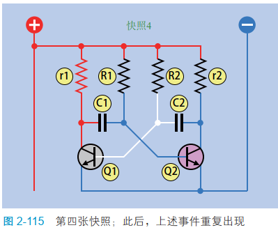
After the fourth snapshot , The situation goes back to snapshot 1 And repeat . If there are other transistors and LED According to the plan 2-111 Connect to the circuit ,LED Should be in snapshot 1 And snapshot 4 Light up in the middle .
Coupling capacitor
As you can see , The oscillator is difficult to understand , And this circuit is very common . actually , use Image search “ oscillator ”, You can easily find this circuit , however , Many people are still puzzled about this .
The key to this circuit is the snapshot 2 And snapshot 4 in , The voltage on one side of the capacitor drops suddenly , The same voltage drop is also produced on the other side —— You are experimenting 9 The coupling effect witnessed in .
But how did the coupling begin ?
Considering that the circuit is basically symmetrical , When you first energize a circuit , Why don't both transistors turn on , Or both transistors are blocked ?
In an ideal situation , Two transistors or resistors can be identical , The initialization of the circuit will be symmetrical . But in fact , There are always some manufacturing errors in resistors and capacitors , So that one transistor always turns on ahead of the other . As soon as this phenomenon occurs , The circuit loses its balance , Thus, the oscillation phenomenon I described earlier appears .
Another question I need to explain is , How to determine which part of the oscillator circuit to obtain the output ? In the original circuit , Please note that r1 and r2 The resistance of is much lower than R1 and R2. This will make C1 The left side of the plate charges quickly , Until the power supply voltage is approached ,C2 The same is true of the right plate of the . therefore , We can measure a wide range of voltage from any of these two points . I selected the measuring point on the left , The reason is simple : It is easier to add components to the circuit diagram at this point .
If the current in the circuit is too high , The charging speed of the capacitor will slow down , It further affects the time setting and balance of the oscillator . therefore , I put the input signal through a 100 kΩ The resistor input to the base of another transistor . The base current of the other transistor is very small , But it amplifies the signal , So you can do something useful with transistors .
Why is it so complicated ?
I think everything is an oscillator circuit , It's a little hard to understand .
Processed pulses
You already know , Two transistors can send out intermittent pulse signals , The third transistor amplifies the signal , by LED Provide electric energy . Think back to the previous experiment , What did you learn from it , It can be applied to this experiment ?
The circuit of this experiment fluctuates very slowly , So we can add... To the circuit RC The Internet , Make it more interesting .
Take a look at the picture 2-116, Newly added RC The network is at the bottom of the diagram .
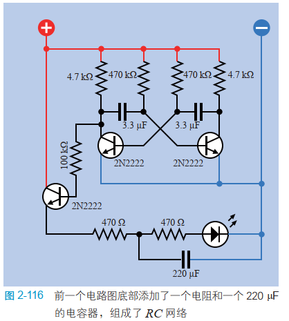
chart 2-117 in , The newly added or changed components are drawn in the lower right corner , Mark in color , The unchanged components are drawn in gray . At this time, the circuit runs ,LED Will pulse slowly , Not on and off . Do you understand why ? The capacitor passes through the first 470 Ω Resistor charging , And discharge through a second resistor . What does it matter ? Let's assume that you are considering making electronic decorations , The adjustment of its flicker or pulse mode is a very important aesthetic element . On an old apple laptop , The logo will have a pulse of light and shade , Without flashing .

Increase speed
How else can I modify this circuit ? You can easily adjust the speed of the circuit . With two 0.33 μF Replace two of the capacitors 3.3 μF The capacitor . The charging speed should be fast 10 times , therefore LED The blinking speed of will also be increased 10 times . Is that it ?
If you further reduce the capacitance of the capacitor to 0.01 μF, What will happen ? The oscillation frequency is greater than per second 50 Time , You will change from the visible frequency domain to the audible frequency domain .
How to change the output of a circuit from visible to audible ? It's simple ! Remove LED、470 Ω Resistors and 220 μF Capacitor , Put on a small loudspeaker 、100 μF Coupling capacitor and 1 kΩ resistor , Pictured 2-118 Shown . A resistor grounds the emitter of a transistor , Because the transistor can only work when the emitter voltage is determined to be lower than the base voltage . The capacitor blocks the DC component of the signal , At the same time, the AC component is allowed to pass through . In the circuit diagram , I only draw the components that have changes . How should they fit on the bread board ? You must be able to figure it out .

Further modification
Now that the circuit has made a sound , How about raising the tone ? Just replace the small resistor or capacitor in the oscillator circuit . You can remove 470 kΩ The resistor , use 220 kΩ resistor ( Or some intermediate resistance ) Replace . Transistors can switch signals a million times per second , Therefore, the increase of oscillator frequency will not exceed the limit of transistor . A signal that oscillates tenthousand times per second sounds very high . If we increase it to 20000 times per second , It is beyond the hearing range of almost all human ears .
So how about changing the tone ?
In the figure 2-119 The top half of the , I use one. 1 μF The new coupling capacitor replaces the original 100 μF Capacitor , Connect it in series with the speaker . After the capacitance value of the capacitor is reduced , Only through higher frequencies ( short pulse ), So that the sound loses some bass resonance .

If you connect a capacitor in parallel at both ends of the speaker , Pictured 2-119 As shown in the lower half of , What will happen ? The opposite will happen , Because the capacitor still passes through the high frequency signal , And let them bypass the speakers . The function of this capacitor is to bypass the capacitor .
There are many simple ways to modify the circuit . If you feel more motivated , You can copy this circuit , Use one part of the circuit to control another part .
Recovery diagram 2-109 Original component value in , The circuit runs slowly at its original speed . then , Use the output of the circuit to supply power to the copy circuit on the bread board , Copy circuit use 0.01 μF The capacitor , Used to generate audio . The total circuit is shown in the figure 2-120 Shown , The original components in the circuit are painted grey , The audio part is at the bottom .

Marked as A The red wire of the has changed its position , So that the lower half of the circuit obtains electric energy from the output of the upper half . Marked as B Red 、 The blue wire is newly added , It is used to fill the gap between buses on the bread board .
If you change the capacitance or resistance of the upper part of the circuit to speed up the oscillation frequency of the lower part of the circuit , What will happen ?
If you put one 220 μF The capacitors are connected at various points ( The upper and lower parts of the circuit ) And the grounding terminal , What's going to happen ? This will not damage any components , So please experiment .
Another option is to go back to figure 2-116 Produced “ Processed pulse ” optical signal , Change the physical connection of components . You can remove the components from the bread board , Make them into a small wearable device .
Background knowledge : Installing the speakers
The diaphragm of the loudspeaker is also called a paper basin , Used to make sound . however , As the speaker oscillates up and down , It sends out sound waves on both sides . Because the two trains of sound waves are opposite to each other , They can easily cancel each other out .
If you add a speaker around the speaker , Focus the front output sound wave , The received speaker output can be greatly increased . For one 1 Inch size small speaker , You can bend a big card , Stick around it , Pictured 2-121 Shown .

A better way is , Install the speaker in the box , There are holes drilled in the box , Allow the sound from the front of the speaker to radiate outward , The closed back of the box absorbs the sound waves from the back of the loudspeaker .
边栏推荐
猜你喜欢

剑指 Offer II 027. 回文链表

网络模型——OSI模型与TCP/IP模型

TCP与UDP

Invalid Navicat scheduled task

C#中如何调整图像大小

"Spatial transformation" significantly improves the quality of ground point extraction of cliff point cloud

PCB board design - automatic layout 2021-10-15

Neural network and deep learning-3-simple example of machine learning pytorch

417-二叉树的层序遍历1(102. 二叉树的层序遍历、107.二叉树的层次遍历 II、199.二叉树的右视图、637.二叉树的层平均值)

【深度学习 轻量型backbone】2022 EdgeViTs CVPR
随机推荐
SCM Project Training
Solving some interesting problems with recurrence of function
@The difference between resource and @autowired annotation, why recommend @resource?
1742. maximum number of small balls in the box
深度学习系列48:DeepFaker
MySQL简单权限管理
C WinForm panel custom picture and text
Analysis of kinsing dual platform mining family virus
洛谷P2839 [国家集训队]middle(二分 + 主席树 + 区间合并)
Neural network and deep learning-3-simple example of machine learning pytorch
三台西门子消防主机FC18配套CAN光端机进行光纤冗余环网组网测试
What are the problems with traditional IO? Why is zero copy introduced?
Debugging mipi-dsi screen based on stm32mp157
Mysql面试-执行sql响应比较慢,排查思路。
c#ColorDialog更改文本颜色和FontDialog更改文本字体的使用示例
Anaconda navigator启动慢的一个解决方法
Runtime - Methods member variable, cache member variable
WebSocket的理解以及应用场景
將數據導入到MATLAB
Machine learning notes linear regression of time series