当前位置:网站首页>Technical introduction - detailed explanation of chip manufacturing process
Technical introduction - detailed explanation of chip manufacturing process
2022-06-26 01:16:00 【Programmer's record】
Manufacturing process
Chip introduction
- species
(1) By nature : Numbers , Analog chip
(2) According to the purpose : Computer , Home appliance , mobile phone , Medical care , Automobile, etc
(3) function :
[1] Thinking function :CPU,NPU,DSP,FPGA,AI;> [2] perceptive function :MEME,sensor
[3] Transfer function : bluetooth ,wifi
[4] function : Power supply chip- PN junction : It has a single conductivity
(1)N Type semiconductor (Negative, Electrons are negatively charged ): Add a small amount of impurity phosphorus / Silicon of antimony / Germanium crystal ,N Type a semiconductor has high electron concentration , Its conductivity is mainly because free electrons conduct electricity .
(2)P Type semiconductor (Positive, Holes are positively charged ): Add a small amount of impurity boron / Silicon of indium / Germanium crystal ,P Type a semiconductors contain high concentrations of “ hole ”(“ amount to ” positive charge ), Become a substance capable of conducting electricity .
(3)PN The knot is made up of a N Type doping region and a P Formed by the close contact of the doped regions , The contact interface is called metallurgical junction interface

Process introduction
- Semiconductor manufacturing is divided into 4 A process : Silicon wafer manufacturing –>IC Design –> The process before chip manufacturing –> Package test
- Several important steps in the chip manufacturing process : oxidation 、 Deposition 、 Photolith 、 etching 、 Ion implantation / Diffusion, etc


Silicon wafer manufacturing
production process
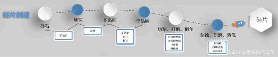
- The raw material is quartz ore , The main component is silica (SiO2).
- Silicon ingot production :
(1) crucible ( Submerged arc furnace , Electric arc furnace ), Usually diameter 12m, The material is graphite , The middle two 3m Long graphite electrodes are used to heat , The melting point of graphite is 3800 Centigrade
(2)(60 Tons of silica + 25 Tons of coal and sawdust ) — 2000 Centigrade —> Silicon liquid — condensation —> 98–99 Pure silicon ingot
[1] Main reaction (1800 Centigrade )––> si And co,
[2] Secondary reaction (1400 Centigrade )––> sic( Third generation semiconductor , Power components )
[3] sic + sio2 ––> si And co- Purification of industrial silicon : With the help of Hydrogen chloride Gas purification
(1)( It is also called Siemens method ) The silicon ingot is crushed into slag 325 High temperature and Hydrogen chloride React ––> H2 And SiHCl3,( impurities : Ferric chloride , Aluminum trichloride , Silicon tetrachloride and other gases ), Silicon trichloride with low boiling point can be separated by controlling the temperature of condenser and distillation tower by using different boiling points of gas
(2) Silicon trichloride is reduced to silicon : stay 1100 It is produced by hydrogen at high temperature of degrees Celsius si, Hydrogen chloride , Silicon tetrachloride . At this temperature , Only silicon is solid , So we can see that the black silicon grows slowly , You can accumulate experience in about a week 250kg Silicon rod ( precision 6 individual 9)
(3) It belongs to polysilicon , The crystal frame structure is not uniform , The whole is composed of many irregular small crystals , It can be used in photovoltaic industry ( Accuracy requirements 6 individual 9)- Polycrystalline silicon to monocrystalline silicon : The mainstream is Chakraskifa , Also called straight drawing method , Tira method ( precision 11 individual 9)
(1) The high-purity polysilicon obtained in the previous step is heated and melted in a crucible made of quartz , Melting point of quartz 1700, Melting point of silicon 1400, Here the temperature is controlled slightly above the melting point of silicon , Then a small strip seed is used as the seed ( Fine monocrystalline silicon ) Immerse in molten liquid , Rotate and pull up slowly to form monocrystalline silicon , Sliced into chip raw materials
(2)8 Inch crystal silicon rod that needs to be pulled slightly , 12 Inch to be pulled , The larger the allocation, the lower the cost- Cutting and grinding chamfer
(1) Diameter grinding : The silicon ingot is cut with a cutting head cone 、 Tail cone 、 And start processing after the quality inspection after cutting , The process includes first accurate alignment of the crystal segments , Then grind the cut crystal cylinder to achieve the required diameter dimension , Finally, add the orientation mark , For large size wafers , Generally, a groove is grinded out of the cylindrical surface as a positioning groove (Notch), For small size, the flat edge is usually ground as the positioning edge (Flat).
[1] Positioning slot / The meaning of locating edges : Help the subsequent process to determine the wafer Wafer Where are you going , In order to locate , The crystal orientation of single crystal growth is also indicated . For subsequent cutting , And testing are convenient . And the cutting position is at the edge , Most of them are also unusable areas .
(2) cutting : The silicon rod is cut into thin silicon wafers with precise geometric dimensions , Silicon powder produced in this process is drenched with water , Waste water and silicon slag will be produced . At the same time, the slice determines wafer Several characteristics of : The thickness of the 、 Slope 、 Parallelism 、 Warpage . The commonly used silicon wafer cutting method is cylindrical cutting 、 Inner circle cutting and carborundum wire cutting .
(3) Chamfering : Abrade wafer Sharp edges and corners around , There are three purposes : prevent wafer Edge rupture 、 Prevent damage caused by thermal stress 、 Add epitaxial layer and photoresist in wafer Flatness of edges .
[1] Generally, one side of the edge surface presents an arc shape after machining (R-type) or T shape (T-type).- Etching, grinding and cleaning
(1) grind : To remove the knife marks on the surface ; Remove the damaged layer ; Improve flatness , send wafer Even in thickness ; Increase surface flatness, etc . At present, the grinding methods are divided into double-sided grinding and surface grinding .
(2) Chemical corrosion : After slicing 、 After grinding and other machining , Due to the stress produced by machining, a certain depth of mechanical stress damage layer will be formed on its surface , And there will be metal ion pollution on the surface . This usually requires a chemical corrosion process to eliminate these effects . The purpose is to produce chemical reaction between acid or alkali solution and silicon wafer at a certain concentration and temperature , Thus, a uniform chemical film is formed on the surface of the silicon wafer .
[1] The total thickness of chemical corrosion removal is generally about 30-50μm.
[2] The commonly used chemical corrosion is acid corrosion or alkali corrosion .
[3] It can greatly eliminate the stress and damage layer caused by wafer back grinding , Thus increasing wafer strength
(3) polishing : The goal of polishing is to remove the fine damage layer on the surface , Get a smooth surface with high flatness . Polishing methods include mechanical polishing and chemical mechanical polishing , Mechanical polishing efficiency is too low , And a large amount of consumables . The speed of chemical mechanical polishing is greatly improved , Surface quality has also improved .
(4) cleaning : Wafer Experience the above processing procedures , Contact with polishing agent in the middle 、 Contamination of abrasives and other chemical reagents and particles , Finally, these impurities need to be removed .Wafer Wet chemical cleaning method is used for cleaning , The most extensive wet chemical cleaning technology is RCA Cleaning .- Wafer evaluation : The wafer needs to be checked according to some parameters specified by the user


Industry barriers
- Main barriers : technology barrier , Certification barriers , Equipment barrier and Capital Barrier .
- technology barrier
(1) Size , Thickness of polishing plate , Warpage of silicon wafer , Resistivity , Curvature , Surface metal residue
(2) The most basic parameter is purity , Is the main technical barrier , Advanced process silicon wafers are required to 9N(99.9999999%)-11N about
(3) Silicon wafers are highly customized products ; Design and manufacture different silicon wafers according to requirements
[1] Silicon wafers are not universal products , Can't copy .
[2] The specifications of large silicon wafers are completely different in each wafer foundry
[3] Different end products have different requirements and specifications for silicon wafers- Certification barriers
(1) The certification process
[1] Provide silicon wafer for trial production ( Most of them are used in test pieces ), Not wafer mass production
[2] Through the test piece, the mass production piece will be produced in small batch
[3] After passing the internal certification, the products will be sent to downstream customers
[4] After customer certification, the supplier of silicon wafer will be finally certified , Sign the contract
[5] The shortest certification cycle for new suppliers also needs 12-18 Months
(2) Silicon wafer suppliers and wafer manufacturers are sticky , It is difficult for new suppliers to break the stickiness- Equipment barriers
(1) The core equipment for manufacturing silicon wafers is the single crystal furnace , It can be said to be a silicon chip “ lithography ”.
(2) The monocrystal furnaces of the international mainstream silicon wafer manufacturers are all made by themselves , Other silicon wafer manufacturers cannot buy .
(3) Other major silicon wafer manufacturers have independent single crystal furnace suppliers , And sign a strict confidentiality agreement , As a result, the external silicon wafer manufacturers cannot buy ( High specification single crystal furnace )- Capital barriers
(1) The manufacturing process is complicated , Need to buy advanced , Expensive production equipment
(2) It needs to be constantly modified and debugged according to the different needs of customers .
(3) Wafer factories have a long certification cycle for silicon wafers , During this period, continuous investment is required
IC Design
Design process

- The design process is divided into two parts ( Process related design can be called back-end design )
(1) Front end design ( Also known as logical design )
(2) Back end design ( Also called physical design )
- The main process of front-end design :
(1) Specification formulation ( Chip specification , Function list )
[1] Customers to chip design companies (Fabless, Fabless design company ) Proposed design requirements
[2] Including the specific function and performance requirements of the chip .
(2) Detailed design , Fabless According to the customer's specifications , Come up with design solutions and specific implementation architecture , Partition module function .
(3)HDL code
[1] Hardware description language (VHDL,Verilog HDL), Industry companies generally use the latter
[2] The hardware description language is used to describe and implement the module functions in code , That is, the actual hardware circuit functions are passed through HDL Language description , formation RTL( Register transfer level ) Code .
(4) Simulation verification , Check the correctness of the coding design
[1] The test standard is (1) Established specifications , Whether it is precisely realized
[2] Design and simulation verification are iterative processes , Until the verification results show that the specifications are fully met .
[3] Simulation verification tool :Modelsim(Mentor), VCS(Synopsys) It can be done to RTL Level code for design verification .
[4] This part is called pre simulation , The simulation after logic synthesis can be called post simulation .
(5) Logic synthesis (Design Compiler)
[1] The result of logic synthesis is to realize the design HDL Translate the code into gate level netlist netlist.
[2] Comprehensive needs to set constraints , It is the area of the circuit that we hope to synthesize , Time series and other target parameters .
[3] Logical synthesis needs to be based on a specific synthesis library , In different libraries , Area of basic standard unit of gate circuit , Timing parameters are different . therefore , The selected comprehensive library is different , The integrated circuit is in time sequence , There are differences in area .
(6)STA( Static time series analysis ), It belongs to the verification category
[1] It mainly verifies the circuit in time sequence , Check whether the circuit violates the set-up time and hold time .
[2] It is the basic knowledge of digital circuit , When these two timing violations occur in a register , Is unable to sample and output data correctly , So the function of digital chip based on register will certainly have problems
(7) Formal verification , It belongs to the verification category
[1] It's functional (STA It's timing ) Verify the integrated netlist .
- Back end design process :
(1)DFT( Design for testability ) The goal is to consider future tests at the time of design
(2) Layout planning (FloorPlan), The macrocell module where the chip is placed , Determine the placement of various functional circuits in general , Such as IP modular ,RAM,I/O Pin, etc .
[1] Layout planning can directly affect the final area of the chip
(3)TS( Clock tree synthesis ), Clock wiring
[1] Due to the global command of clock signal in digital chip , Its distribution should be symmetrical and connected to each register unit , Thus, when the clock reaches each register from the same clock source , Minimum clock delay difference .
(4) wiring (Place & Route), Common signal wiring
[1] Including various standard units ( Basic logic gate circuit ) The routing between . hear 0.13um,90nm The process is actually the minimum width that the metal wiring can reach here , From the microscopic point of view, it is MOS Channel length of the pipe .
(5) Parasitic parameter extraction
[1] Analyze signal integrity issues , Avoid signal distortion errors
[2] reason : Mutual inductance between adjacent conductors , The coupling capacitor will produce signal noise inside the chip , Crosstalk and reflection . These effects can cause signal integrity problems , Cause signal voltage fluctuation and change
(6) Physical verification of layout , Verify the function and timing of the physical layout of the completed wiring
[1] The physical layout is based on GDSII Send the file format to the chip foundry
- Chip design company
- Chip architecture


Industry barriers
- IC The design industry is a technology and capital intensive industry .
- technology barrier
(1)IC For reliability 、 stability 、 The integration and other performance indicators have high requirements . Complex systems need to provide slave chips 、 Comprehensive technical support from application circuit to system software .IC The design company needs to master the application characteristics of various components and the supporting software and hardware technology , You also need to be familiar with the technical background of the product application 、 System integration interface 、 Production process 、 Site environment and other key characteristics , These are based on technology accumulation and industry experience .
(2)IC Its design and production technology have developed rapidly , During development and production , It is necessary to keep up with the development trend of international advanced technologies and processes , Optimize the process design and production arrangement , To gain an advantage in the competition .- Capital and scale barriers
(1)IC The product of the design enterprise must reach a certain capital scale and business scale , In order to obtain the space for survival and development through the scale effect .IC The design industry has high mass production standards , There are high standards of economies of scale . The investment in chip R & D is huge , The unit price is low , Therefore, the sales volume needs to be up to millions to achieve profit and loss balance .
(2) As the electronic product market changes rapidly 、IC The design and development cycle is long and the uncertainty of success is large , It often happens that the long design cycle leads to the collapse of the company , Or the designed products have not met the requirements of the target market . therefore , Capital and scale are important barriers to the industry .- Talent barrier
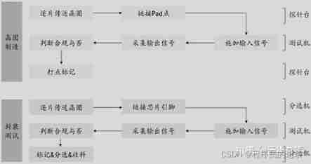
Chip making && Package test
Manufacturing process

- The previous process is divided into two parts : Wafer processing , Wafer needle test
(1) Wafer processing process : It mainly produces circuits and electronic components on the wafer ( Transistors / Capacitor / Logic gates, etc )
(2) Wafer stylus process : Test its electrical characteristics by needle measuring instrument , Nonconformities will be marked- Photolith
(1) First lithography (N+ Buried diffusion hole )
(2) Epitaxial layer deposition : Vapor phase epitaxial growth of silicon (VPE), oxidation
(3) Second lithography (P+ Isolate the diffusion hole )
(4) Third lithography (P Type base diffusion hole )
(5) The fourth lithography (N+ Emission area diffusion hole )
(6) The fifth lithography ( Lead contact hole )
(7) The sixth lithography ( Wire inside the metal painting : Reverse engraved aluminum )- cleaning technology
- Optical development
(1) The process of exposure and development on a photosensitive adhesive , Convert the pattern on the mask to the film layer or silicon crystal under the photoresist . Mainly including photosensitive adhesive coating , bake , The hood is aligned , Exposure and development procedures
(2) Exposure mode : Ultraviolet (uv) ,X ray , electron beam , Extreme ultraviolet- Etching technology
(1) The technique of removing materials by chemical reaction and physical impact
(2) Wet etching ( Chemical solution )
(3) Dry etching ( Plasma etching )- Deposition
(1) Chemical vapor deposition (CVD): Introduce two or more gaseous raw materials into the reaction chamber , There is a chemical reaction between them , Form a new material , Deposited on the wafer surface .
[1] For depositing a wide range of insulating materials 、 Most metal materials and metal alloy materials .
[2] common CVD Thin film : 2. Vaporized silicon ( Oxide layer ), Silicon nitride , Polysilicon, etc
(2) Physical vapor deposition (PVD): Means in vacuum , A thin film preparation technique in which a material is deposited on a plated workpiece by physical means .
[1] It is mainly divided into three categories : Vacuum evaporation coating 、 Vacuum sputter plating and vacuum ion plating- Ion implantation : The dopant can be implanted into a specific area of a semiconductor component in an ionic form , To obtain accurate electronic characteristics , The ions must first be accelerated to have sufficient energy and velocity , To penetrate ( implant ) Thin film , Reach the predetermined implantation depth .
- Chemical mechanical polishing : It is a processing technology combining chemical corrosion and mechanical removal , It is the only technology in machining that can realize the global planarization of the surface . Conducive to subsequent film deposition .
- Hood detection : The mask is a quartz plate with high precision , It is used to make the electronic circuit image on the wafer , To facilitate the production of integrated circuits . The hood detector is a combination of image scanning technology and advanced image processing technology , Capture the missing on the image .


Package test

- Wafer cutting : Cut and separate the grains of the wafer processed by the pre process .
- Welding wire
(1)IC The fabrication process is to use plastic or ceramic packaging grains and wiring to form integrated circuits , The purpose is to make the protective layer of the circuit , Avoid mechanical scratch or high temperature damage to the circuit . Finally, the entire integrated circuit will be pulled out of the scaffold (Pin), Call it stringing , Used for connecting with external circuit board .- Sealant : The purpose is to prevent moisture from invading from the outside 、 Mechanically support the conductors 、 Removal of internal heat generation and provision of a hand-held form .
(1) The process : Place the conductor rack on the frame and preheat , Then place the frame on the assembly die on the die press , Then fill with resin and wait for hardening .- shear / Take shape
(1) shear : The purpose is to separate the grains assembled on the wire rack independently , And remove unnecessary connecting materials and some protruding resins .
(2) Take shape : The purpose is to press the outer pins into various pre designed shapes , So that the device can be used on the circuit board .- Testing and inspection : Ensure the quality of the packaged chip , Ensure the yield .
Industry barriers
- brief introduction : It is a technology intensive and capital intensive industry , In technology 、 personnel 、 Customer resources 、 Money 、 There are high barriers to entry in industrial integration .
- technology barrier :
(1) Covering many disciplines , Including computers 、 automation 、 signal communication 、 Electronics and microelectronics , It is typically technology intensive 、 Knowledge intensive high-tech industries .
(2) reliability 、 High stability and consistency requirements
(3) Chip products continue to be upgraded iteratively , The test equipment also needs to cope with the increasing requirements for test parameters, functions and efficiency .- Talent barrier
(1) R & D personnel : Not only does it require multidisciplinary expertise , It also needs many years of practical work and the experience of senior technicians “ Pass on 、 help 、 belt ” Next , To complete the knowledge reserve and professional experience ;
(2) Management talent : You need to have rich experience in this field , Be familiar with the operation rules of the industry , Grasp the cycle fluctuation of the industry , To specify the development strategy in line with the development stage of the enterprise ;
(3) Market development and sales talents : It also requires considerable technical foundation and rich industry experience , In order to be able to 、 Accurately deliver the technical characteristics of the company's products and the technical requirements of customers , The training cycle of mature salespeople is long .- Capital and scale barriers
(1) Keep the technology progressiveness 、 Leading technology and market competitiveness of products , The investment in technology research and development is increasing .
(2) The products of the enterprise must reach a certain capital scale and business scale , To get the space for survival and development
(3) From R & D project initiation 、 Trial production 、 verification 、 Optimize 、 Higher labor costs and R & D expenses are required in all links from marketing to sales .
(4) There are many categories of semiconductor products , The market changes rapidly 、 The performance parameters are different , Cash flow is required to support the enterprise's long-term R & D investment and long-term customer certification investment .- Industrial Synergy barriers
(1) stay Fabless In mode , Industrial Synergy barriers are mainly reflected in test equipment enterprises 、 Semiconductor upstream design enterprise 、 Wafer manufacturing enterprises and packaging and testing enterprises have established stable and close cooperative relations . In the context of Industrial Synergy , The early investment of the enterprise is large , Collaborative accumulation takes quite a while .
(2) The Industrial Synergy established and stably operated by the advanced market entrants will constitute a major barrier for them to enter the industry .- Customer resource barriers
(1) The accumulation of customer resources requires a long time of market cultivation , Before getting an order , The certification cycle is long , The customer certification cycle is 6-36 Months .- Chip making & test & Packaging company

Nine core equipment
- Nine major equipment
(1) equipment : Oxidation diffusion machine , Film deposition equipment , lithography , Glue applicator , Etching machine , Ion implanter ,CMP Polishing equipment , Testing equipment , Cleaning machine
(2) The increase in the market size of front-end devices is due to chip materials / structure / The process tends to be complex
[1] Type of material :Poly-Si, tungsten , aluminum –> tungsten , copper –> tungsten , copper , cobalt --> The new material
[2] Structural technology : 2D Plane structure –> FinFet structure --> GAAFet structure
[3] Process technology : Photolithography –> Multi graphic process –> Deep UV EUV+ Multi graphic process
(3) Moore's law continues (Soc + SiP)
[1] Semiconductors are not far from the limit of process miniaturization , Channel front channel device to improve transistor density
[2] Soc System level chips : Fin transistor FET It's the realization of 7nm The key technology of
[3] 3D Chip manufacturing technology : from IC From the design point of view, integrate the three-dimensional structure chip to improve the efficiency
[4] SiP Systematic encapsulation : The key technology to improve chip performance from the perspective of packaging
(4) Enterprise and share
(5) Domestic equipment enterprises and manufacturing processes- Photolith / Etching /CVD Three items of equipment
(1) The largest market
(2) Key technology nodes
(3) lithography
[1] Unit price and structure diagram of equipment
[2] Core components of equipment : The light source , objective lense , Precision control system
[3] ArF Immersive UV (14nm) to EUV Extreme ultraviolet light (< 10nm
)
![> [2] 3D Chip manufacturing technology](/img/d2/a7d09ae722280f9bf482e12bee98cb.jpg)


(4) Under the trend of chip process miniaturization , The investment and difficulty increase the most

- PVD/ cleaning / The market scale of measuring equipment is in the second echelon

Reference documents
(1) Numbers IC Introduction to the whole design process
(2)IC Enterprise description
(3) Introduction to core equipment
(4) Semiconductor front device industry research
(5) Basic chip manufacturing process
边栏推荐
- Flex & bison start
- Chapter V exercises (124, 678, 15, 19, 22) [microcomputer principles] [exercises]
- Endnote IEEE TRANSACTIONS ON INDUSTRIAL ELECTRONICS/TIE/TPEL 参考文献格式模板
- Balanced binary tree AVL
- Android cache usage tool class
- Making 3D romantic cool photo album [source code attached]
- Redis之Strings命令
- Sqlserver is case sensitive
- 新库上线 | CnOpenData农产品批发价格数据
- .net使用Access 2010数据库
猜你喜欢

QT cmake pure C code calls the system console to input scanf and Chinese output garbled code
Qt Cmake 纯C 代码调用系统控制台输入scanf 及 中文输出乱码

Error 65:access violation at 0x58024400: no 'read' permission

The maze of God's perspective in robot vision

在线小工具分享(不定时更新,当前数量:2)

RT-Thread 项目工程搭建和配置--(Env Kconfig)

从查询数据库性能优化谈到redis缓存-谈一谈缓存的穿透、雪崩、击穿

Multiple interface calls, using promise all、Promise. Race and promise any

新库上线 | CnOpenDataA股上市公司IPO申报发行文本数据

Zhihuijia - full furniture function
随机推荐
Musk vs. jobs, who is the greatest entrepreneur in the 21st century
ciscn_ 2019_ en_ two
Radio boxes are mutually exclusive and can be deselected at the same time
Web信息收集,互联网上的裸奔者
案例:绘制Matplotlib动态图
Idea configuration
Balanced binary tree AVL
数据分析——切片器、数据透视表与数据透视图(职场必备)
Android cache usage tool class
C disk cleaning strategy of win10 system
. user. PHP website installation problems caused by INI files
Return value is object type method call equals()
Case: drawing Matplotlib dynamic graph
Computer network knowledge summary (interview)
When you run the demo using the gin framework, there is an error "listen TCP: 8080: bind: an attempt was made to access a socket in a way forbidden"
Post ordered clue binary tree
Sqlserver is case sensitive
Enlightenment Q & A
containerd客户端比较
jarvisoj_ level2_ x64