当前位置:网站首页>i. MX - rt1052 pulse width modulation (PWM)
i. MX - rt1052 pulse width modulation (PWM)
2022-06-21 12:13:00 【Summer foam and light rain】
Write it at the front :
The purpose of this article is to summarize backup 、 For future reference , Because it's a personal summary , If there is any wrong , Welcome to correct ; in addition , Most of the content comes from the Internet 、 Books 、 And all kinds of manuals , In case of infringement, please inform , Immediately delete the post and apologize .
Catalog
General module diagram

Some features
- 16 Bit resolution , Support Center 、 Edge aligned and asymmetrical PWMs Three comparison modes
- PWM The outputs can be used as complementary pairs or as independent channels
- Be able to accept signed numbers to produce PWM
- Independently control each PWM Two edges of the output
- Support with external hardware or other PWM Sync
- Double buffering PWM register
- The overall reload rate is from 1 To 16
- Half cycle Heavy load capacity
- Every PWM The cycle can generate multiple output trigger events by hardware
- Dual switch support PWM Output
- Fault inputs can be assigned to control multiple PWM Output
- Programmable filter for fault input
- Independently programmable PWM Output polarity
- Separate top and bottom deadband inserts
- Every PWM The outputs are controlled by separate software
- PWM_X The pin can choose to output the third... From each sub module PWM The signal
- Not used PWM The generated channel can be used for input capture function
The above listed features are commonly used , Please refer to the manual for other features
Clock selection

As shown in the figure above , Each sub module can choose between three clock signals :IPBus The clock 、EXT_CLK and AUX_CLK.EXT_CLK The clock points to all sub modules . AUX_CLK Input signal from sub module 0 radio broadcast , And it can be selected as the clock source by other sub modules , So that sub modules 0 Of 8 Bit prescaler and MCTRL[RUN] All sub modules can be controlled . After selecting the clock source, it can only be used as a after frequency division FLEXPWMx_PWM0/1/2/3 Counting clock of sub module , The frequency division value is determined by 8 Bit register CTRL[PRSC] Select prescaler divisor .
About EXT_CLK The clock explains :
This signal allows PWM An external source ( Usually a timer or chip ) control PWM The clock . In this way ,PWM It can be synchronized with the timer , Or multiple chips can be synchronized with each other .
PWM Output
RT1052 have 4 individual eFlex PWM(eFlex_PWM1~eFlex_PWM4), Every eFlexPWM It has four channels . Yes PWM_A、 PWM_B and PWM_X There are three types , Only one eFlex_PWM1 Yes, there is PWM_X This type of , The other three are not ;PWM_A And PWM_B It can be output independently or as a complementary pair .
Each sub module FLEXPWMx_PWM0/1/2/3, Have 6 Compare registers , this 6 The comparison registers are divided into 3 Group ; Two comparators and correlation VALx Registers are used for each PWM The output signal ; A comparator and VALx Register is used to control the opening edge , And the other comparator and VALx The register is used to control the closing edge . Here's the picture :

After passing the above figure 6 Compare registers (3 Group comparator ) After control output , Then it is transformed into... Through some configurations in the following figure PWM_A、 PWM_B and PWM_X These three types of output ( See the general module diagram for details ):

Independent and complementary functions
towards CTRL2 [INDEP] Write logic 1 Will be a pair of PWM The output is configured as two independent PWM passageway ; Every PWM Output by its own VALx Control over , The VALx Run on independent of other outputs .
Logic 0 write in CTRL2 [INDEP] Will PWM The output is configured as a pair of complementary channels . As shown in the figure below , In complementary channel operation , When PWM The pins are well matched , Which signal is connected to the output pin (PWM23 or PWM45) from MCTRL[IPOL] decision .

Alignment mode
PWM The timer of each sub module of the counts up only , Then reset to INIT value .
1、 Center alignment

As you can see from the diagram , Two values must be specified ( Open and close edges ), Instead of using a single value to determine the pulse width , The output pulse width is determined by these two values ( Take the range value ); And what kind of (PWM_A、 PWM_B or PWM_X) type , Is corresponding to VALx Register set determined .
2、 Edge alignment
When the opening edge of each pulse is specified as INIT When the value of , An edge alignment operation will occur , As shown in the figure below . therefore , It is only necessary to change the pulse width by periodically updating the corresponding off edge value ( That is, the pulse width is INIT It's worth it VALx Register controlled off edge value ).

Frequency overflow calculation
flexPWM It's a 16 Bit peripheral , So the maximum count interval is 0 ~ 65536, Note that the interval is used here because it can accept signed numbers to generate PWM Of ; In general , Yes IPBus Of the clock , Its clock source is IPG clock, from AHB clock Divided frequency .
Let's assume that pwm The use of ipgclk The frequency of is 132MHz, And the frequency division value is 1, Set up pwm The signal frequency is 1KHz, That is to say 132MHz /1 /1KHz = 132000 > 2^16; That is, overflow .
Deadband insertion
Deadband insertion , It is similar to the delay operation , The dead zone insertion logic control diagram of each sub module is as follows :

Dead time register (DTCNT0 and DTCNT1) Specifies... For dead time delay IPBus Number of clock cycles . Each time the deadtime generator input changes the State , Will insert the dead time . Dead time will be two of a pair PWM The output is forced to an invalid state .
Dead time insertion diagram :
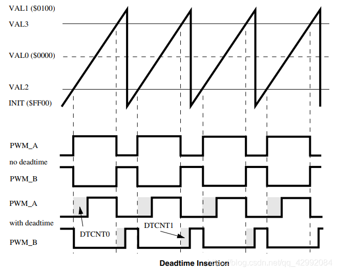
PWM Complementary pairs are often used to control half bridge drive circuits , Here's the picture :

When using deadband free complementarity pwm When controlling the bridge drive circuit ,PWM_A 、PWM_B Control such as no deadtime Schematic diagram . In theory , The same is true of the switch state that controls the drive circuit , But in practical application, the transistor controlled by the driving circuit switch is not ideal , It takes time for a transistor to change from an off state to an on state or from an on state to an off state ; And usually the opening time is different from the deadline . If you do not insert the dead time , When PWM When the state changes, the upper and lower transistors are likely to be turned on at the same time , This causes a short circuit in the circuit .
When using complementarities that add dead zones PWM when ,PWM_A 、PWM_B Control such as with deadtime Schematic diagram , At this time, due to the dead time (DTCNT0) The existence of , Look at the dead band waveform above ,PWM_A Keep the low level unchanged , After the dead time ( In this time period PWM_B The controlled transistor has been able to complete the state transition ) PWM_A To high level , The upper transistor is on , The lower transistor has completely turned off , In this way , By analogy , Selecting the appropriate dead time will prevent short circuit .
Demo code
#include "bsp_pwm.h"
#include "pin_mux.h"
#include "board.h"

#include "fsl_xbara.h"
#include "fsl_debug_console.h"


/*  Whether to use  FlexPWM Fault protection function  */
#define FAULT_PROTECTION_ENABLE 0

/* The PWM base address */
#define BOARD_PWM_BASEADDR PWM1

void PWM_Signals_Update(void)
{

    static uint32_t pwmVal = 4;

    pwmVal = pwmVal + 4;

    /* Reset the duty cycle percentage */
    if (pwmVal > 100)
    {

        pwmVal = 4;
    }

    /* Update duty cycles for PWM signals */
    PWM_UpdatePwmDutycycle(BOARD_PWM_BASEADDR, kPWM_Module_3, kPWM_PwmA, kPWM_SignedCenterAligned, pwmVal);

    /* Set the load okay bit for all submodules to load registers from their buffer */
    PWM_SetPwmLdok(BOARD_PWM_BASEADDR, kPWM_Control_Module_3, true);
}

/** * @brief This function is PWM Signals Config * @return none */
static void PWM_Signals_Config(void)
{

    uint16_t deadTimeVal = 0;
    pwm_signal_param_t pwmSignal[1];
    uint32_t pwmSourceClockInHz;
    uint32_t pwmFrequencyInHz = 1000;		// PWM signal frequency

    pwmSourceClockInHz = CLOCK_GetFreq(kCLOCK_IpgClk);		//  Get the clock frequency

    pwmSignal[0].pwmChannel       = kPWM_PwmA;
    pwmSignal[0].level            = kPWM_HighTrue;
    pwmSignal[0].dutyCyclePercent = 50; /* 1 percent dutycycle */
    pwmSignal[0].deadtimeValue    = deadTimeVal;			//  Deadband value ; Use only if the channel pair is working in a complementary manner
    pwmSignal[0].faultState       = kPWM_PwmFaultState0;	//  Fault status

    /*  To configure  PWM1_PWM3_A; The center of the symbol is aligned ;PWM The signal frequency is  pwmFrequencyInHz */
    PWM_SetupPwm(BOARD_PWM_BASEADDR, kPWM_Module_3, pwmSignal, 1, kPWM_SignedCenterAligned, pwmFrequencyInHz,
                 pwmSourceClockInHz);

    /* Set the load okay bit for all submodules to load registers from their buffer */
    PWM_SetPwmLdok(BOARD_PWM_BASEADDR, kPWM_Control_Module_3, true);

    /* Start the PWM generation from Submodules 3 */
    PWM_StartTimer(BOARD_PWM_BASEADDR, kPWM_Control_Module_3);
}

/** * @brief This function is PWM all Config * @return none */
void PWM_Config(void)
{

    /* Structure of initialize PWM */
    pwm_config_t pwmConfig;
    pwm_fault_param_t faultConfig;

/*  Only when  pwm No error input or error detection is prohibited before normal output  pwm wave  */
#if (0 == FAULT_PROTECTION_ENABLE)
    /*  Error detection is prohibited  */
	BOARD_PWM_BASEADDR->SM[kPWM_Fault_3].DISMAP[kPWM_faultchannel_0] = 0;	//  Here we need to correspond to  PWM Sub module channel of

#else
    /* Set the all PWM Fault inputs to a high value */
    XBARA_Init(XBARA1);
	/*  Set up  pwm The error input is high , No mistakes  */
    XBARA_SetSignalsConnection(XBARA1, kXBARA1_InputLogicHigh, kXBARA1_OutputFlexpwm1Fault0);
    XBARA_SetSignalsConnection(XBARA1, kXBARA1_InputLogicHigh, kXBARA1_OutputFlexpwm1Fault1);
    XBARA_SetSignalsConnection(XBARA1, kXBARA1_InputLogicHigh, kXBARA1_OutputFlexpwm1234Fault2);
    XBARA_SetSignalsConnection(XBARA1, kXBARA1_InputLogicHigh, kXBARA1_OutputFlexpwm1234Fault3);

#endif /* FAULT_PROTECTION_ENABLE */

    /* * config.enableDebugMode = false; // true:PWM Continue to run in debug mode ;false:PWM Pause in debug mode  * config.enableWait = false; // true:PWM Continue to  WAIT mode ;false:PWM stay  WAIT Pause in mode  * config.reloadSelect = kPWM_LocalReload; // PWM The module reloads the register using a local reloading signal  * config.clockSource = kPWM_BusClock; //  Choose the clock source  * config.prescale = kPWM_Prescale_Divide_1; //  Set clock division  * config.initializationControl = kPWM_Initialize_LocalSync;//  Local synchronization results in reinitialization  * config.forceTrigger = kPWM_Force_Local; //  Select force update signal  * config.reloadFrequency = kPWM_LoadEveryOportunity; //  choice  PWM Automatic reload frequency  * config.reloadLogic = kPWM_ReloadImmediate; //  Once set LDOK position , The buffer register will load the new value  * config.pairOperation = kPWM_Independent; // PWM A and PWM B Operate as two independent channels  */
    PWM_GetDefaultConfig(&pwmConfig);

    /* PWM clock select */
    pwmConfig.clockSource = kPWM_BusClock;						//  Choose as  IPBus clock
    /* The Prescaler divides frequency */
    pwmConfig.prescale = kPWM_Prescale_Divide_8;				//  Set clock division   choose  IPBus After clock ,PWM clock = IpgClk/Div
    /* Use full cycle reload */
    pwmConfig.reloadLogic = kPWM_ReloadPwmFullCycle;			//  Full cycle update
    /* PWM A & PWM B operate as 2 independent channels */
    pwmConfig.pairOperation   = kPWM_Independent;				// PWMA,PWMB Output independently
    pwmConfig.enableDebugMode = true;							//  Enable to work in  DEBUG Pattern

    /* Initialize submodule 3 */
    if (PWM_Init(BOARD_PWM_BASEADDR, kPWM_Module_3, &pwmConfig) == kStatus_Fail)
    {

        PRINTF("PWM initialization failed\n");
        return;
    }

#if FAULT_PROTECTION_ENABLE
    /* * config->faultClearingMode = kPWM_Automatic; * config->faultLevel = false; * config->enableCombinationalPath = true; * config->recoverMode = kPWM_NoRecovery; */
    PWM_FaultDefaultConfig(&faultConfig);

#if (defined(FSL_FEATURE_PWM_FAULT_LEVEL_HIGH) && FSL_FEATURE_PWM_FAULT_LEVEL_HIGH)
    faultConfig.faultLevel = true;
#endif

    /* Sets up the PWM fault protection */
    PWM_SetupFaults(BOARD_PWM_BASEADDR, kPWM_Fault_0, &faultConfig);
    PWM_SetupFaults(BOARD_PWM_BASEADDR, kPWM_Fault_1, &faultConfig);
    PWM_SetupFaults(BOARD_PWM_BASEADDR, kPWM_Fault_2, &faultConfig);
    PWM_SetupFaults(BOARD_PWM_BASEADDR, kPWM_Fault_3, &faultConfig);

    /* Set PWM fault disable mapping for submodule 0/1/2/3 */
    PWM_SetupFaultDisableMap(BOARD_PWM_BASEADDR, kPWM_Module_0, kPWM_PwmA, kPWM_faultchannel_0,
                             kPWM_FaultDisable_0 | kPWM_FaultDisable_1 | kPWM_FaultDisable_2 | kPWM_FaultDisable_3);
    PWM_SetupFaultDisableMap(BOARD_PWM_BASEADDR, kPWM_Module_1, kPWM_PwmA, kPWM_faultchannel_0,
                             kPWM_FaultDisable_0 | kPWM_FaultDisable_1 | kPWM_FaultDisable_2 | kPWM_FaultDisable_3);
    PWM_SetupFaultDisableMap(BOARD_PWM_BASEADDR, kPWM_Module_2, kPWM_PwmA, kPWM_faultchannel_0,
                             kPWM_FaultDisable_0 | kPWM_FaultDisable_1 | kPWM_FaultDisable_2 | kPWM_FaultDisable_3);
    PWM_SetupFaultDisableMap(BOARD_PWM_BASEADDR, kPWM_Module_3, kPWM_PwmA, kPWM_faultchannel_0,
                             kPWM_FaultDisable_0 | kPWM_FaultDisable_1 | kPWM_FaultDisable_2 | kPWM_FaultDisable_3);

#endif /* FAULT_PROTECTION_ENABLE */

    /* PWM signals config */
    PWM_Signals_Config();
}


/*---------------------------- END ----------------------------*/
边栏推荐
猜你喜欢

STM32笔记之 PWM(脉宽调制)

HMS core machine learning service ID card identification function to achieve efficient information entry

Knowledge points: several special wiring methods for PCB

巨头局终战:即时零售

Adapter power supply automatic test equipment | introduction to charger ATE test system nsat-8000

Vs code + GCC environment compilation for STM32 development

南京大学 静态软件分析(static program analyzes)-- Intermediate Representation 学习笔记

Hands on data analysis data reconstruction
Golang implements redis (9): use geohash to search people nearby

Introduction to common source oscilloscope software and RIGOL oscilloscope upper computer software ns-scope

随机推荐
站在数字化风口,工装企业如何“飞起来”
Tensorflower使用指定的GPU和GPU显存
STM32笔记之 SWJ(JTAG-DP和 SW-DP)
Chapter VIII web project testing
Centos7 升级MySQL5.6.40至企业版5.6.49
Is it safe to hit new bonds with one click? Is it reliable?
MySQL-DDL
I would like to ask you guys, the flick CDC will add a table level exclusive lock before extracting the full amount of Oracle data
Rename all files in the folder with one click
Nanjing University static program analyses -- intermediate representation learning notes
MySQL-DQL
『忘了再学』Shell流程控制 — 36、for循环介绍
Understand UML class diagram and sequence diagram
Typescript variable declaration - type assertion
Use praise to improve performance 
i.MX - RT1052时钟及锁相环(PLL)分析
Redis里5种基本数据类型常用指令
matrial3d参数分析
Flink tuning (I) resource tuning and back pressure analysis
Hands on data analysis data reconstruction