当前位置:网站首页>Operational amplifier - Notes on rapid recovery [II] (application)
Operational amplifier - Notes on rapid recovery [II] (application)
2022-07-24 11:26:00 【It is said that this is ZZY】
Operational amplifier —— Quick recovery notes [ Ii. ]( Application articles )
List of articles
Please refer to the previous article in the column before reading , Learn the basics .
The resource acquisition
The reason for writing this article is that I often forget how to use op amp , It is hoped that through several examples and analysis, it can be analyzed quickly and in detail . Part of the circuit simulation and circuit simulation software , I have uploaded it to the cloud disk , Here we recommend Alibaba cloud disk , Downloading without speed limit is fast , Download address . Extraction code : 00kx.
Pre knowledge
Kirchhoff's law
Kirchhoff's current law Also called KCL. It means that the current flowing in at any node in the circuit is equal to the current flowing out , That is, the algebraic sum of the current on the node is 0.

node : The branch point of a circuit . ad locum , You can close any curve or surface , As a generalized node . Like mechanical mass , Objects can be abstracted into particles for analysis .

Simply put, you can draw a circle directly , For this circle , This circle is a node , The current entering and leaving this circle is combined into 0.
Zener diode / Zener diode /Zener diode
The characteristic of Zener diode is after breakdown , The voltage at both ends remains basically unchanged . This voltage is often said in the manual Nominal Zener Voltage, Nominal stabilized voltage . such , When the voltage regulator is connected to the circuit , If the supply voltage fluctuates , When the voltage of each point in the circuit changes due to other reasons , The voltage at both ends of the load will remain basically unchanged .
Its reverse characteristic is when the reverse voltage is lower than the reverse breakdown voltage , The reverse resistance is very large , The reverse leakage current is very small . however , When the reverse voltage approaches the critical value of the reverse voltage , The reverse current increases suddenly , It's called breakdown , At this critical breakdown point , The reverse resistance suddenly drops to a very small value . Although the current varies over a wide range , The voltage at both ends of the diode is basically stable near the breakdown voltage , Thus, the voltage stabilizing function of the diode is realized . The key point of its principle is that the resistance is very small when it passes the regulated value , Even with different voltages , The current flowing will not make the voltage at both ends change greatly , This achieves the effect of voltage stabilization .

main parameter
Steady voltage (Uz)
It refers to the stable voltage value generated at both ends when the zener diode passes through the rated current . This value changes slightly with the working current and temperature . Due to differences in manufacturing processes , The voltage stabilizing value of the same type of Zener diode is not completely consistent . for example ,2CW51 Type zener diode Vzmin by 3.0V, Vzmax Then for 3.6V.
Rated current (Iz)
It refers to the current value passing through the tube when the zener diode generates a stable voltage . Below this value , Although the zener diode is not unable to stabilize voltage , But the voltage stabilizing effect will become worse ; Above this value , As long as the rated power loss is not exceeded , It's also allowed , And the voltage stabilizing performance will be better , But consume more electricity .
Dynamic resistance (Rz)
It refers to the ratio of voltage change and current change at both ends of the zener diode . The ratio varies with the working current , Generally, the greater the working current , The smaller the dynamic resistance . for example ,2CW7C The working current of the zener diode is 5mA when ,Rz by 18Ω; The working current is 1OmA when ,Rz by 8Ω; by 20mA when ,Rz by 2Ω ; > 20mA Then basically maintain this value .
Rated power consumption (Pz)
Determined by the allowable temperature rise of the chip , Its value is stable voltage Vz And maximum allowable current Izm The product of the . for example 2CW51 Zener diode Vz by 3V,Izm by 20mA, Then... Of the pipe Pz by 60mWo.
Reverse leakage current (IR)
Refers to the leakage current generated by the zener diode under the specified reverse voltage . for example 2CW58 Zener diode VR=1V when ,IR=O.1uA; stay VR=6V when ,IR=10uA.
Operational Amplifier Applications
Premise :
- Deficiency :
V i n + = V i n − Vin_+ = Vin_- Vin+=Vin−
- Virtual break :
I i n + = I i n − = 0 Iin_+ = Iin_- = 0 Iin+=Iin−=0
application 1
Inverse proportional operation circuit
Here we first put the circuit , Before reading this article, please go to the parameter article , Basic knowledge of operational amplifier . See the column :

V1 Yes, the power output of the amplifier is +5V Of DC voltage .
V2 Is the virtual ground voltage , It is used to simulate the situation without direct grounding . Here is a 2V Of DC voltage
V3 It's a sine wave , Its parameters are as follows :

Reverse amplification derivation :
Deficiency :
V + = V − = V G N D V G N D by V − and V + Value V_+ = V_- = V_{GND}\\ V_{GND} by V- and V+ Value V+=V−=VGNDVGND by V− and V+ Value
Virtual break : Take the inverse input as the node to analyze .
V i n − V G N D R 2 = V G N D − V o u t R 3 K C L Method deduce that the current is equal 、 In the opposite direction , With V G N D To V o u t Positive direction . \frac{V_{in} - V_{GND}}{R_2}= \frac{V_{GND} - V_{out}}{R3}\\ KCL Method deduce that the current is equal 、 In the opposite direction , With V_{GND} To V_{out} Positive direction . R2Vin−VGND=R3VGND−VoutKCL Method deduce that the current is equal 、 In the opposite direction , With VGND To Vout Positive direction .
Simplify to :
V o u t = V G N D ( 1 + R 3 R 2 ) − V i n R 3 R 2 V_{out} = V_{GND}(1+\frac{R_3}{R_2}) - V_{in}\frac{R_3}{R_2} Vout=VGND(1+R2R3)−VinR2R3
Let's try to deduce into , In the above case ,Vout What is the output result of :
V o u t = V G N D ( 1 + R 3 R 2 ) − V i n R 3 R 2 = 2 ∗ ( 1 + 1.5 ) − V i n ∗ 1.5 among V i n = [ 0 , 2 ] , And for sin x wave form give the result as follows : V o u t = [ 2 , 5 ] V_{out} = V_{GND}(1+\frac{R_3}{R_2}) - V_{in}\frac{R_3}{R_2}=2*(1+1.5) - V_{in}*1.5\\ among V_{in}=[0,2], And for \sin{x} wave form \\ give the result as follows :V_{out}=[2,5] Vout=VGND(1+R2R3)−VinR2R3=2∗(1+1.5)−Vin∗1.5 among Vin=[0,2], And for sinx wave form give the result as follows :Vout=[2,5]
The simulation results are as follows :

Special case of reverse amplification
You can see the input of our amplifier in the figure below + The next thing is GND, This is a special case , Corresponding input + The next thing is GND The voltage is 0, Let's try again with the above analysis method :

The following conditions are also met :
Deficiency :
V + = V − = V G N D = G N D A = 0 V G N D by V − and V + Value V_+ = V_- = V_{GND} = GNDA =0\\ V_{GND} by V- and V+ Value V+=V−=VGND=GNDA=0VGND by V− and V+ Value
Virtual break :
V i n − V G N D R 2 = V G N D − V o u t R 3 K C L Method deduce that the current is equal 、 In the opposite direction , With V G N D To V o u t Positive direction . \frac{V_{in} - V_{GND}}{R_2}= \frac{V_{GND} - V_{out}}{R3}\\ KCL Method deduce that the current is equal 、 In the opposite direction , With V_{GND} To V_{out} Positive direction . R2Vin−VGND=R3VGND−VoutKCL Method deduce that the current is equal 、 In the opposite direction , With VGND To Vout Positive direction .
Simplify to :
V o u t = − V i n R 3 R 2 V_{out} = -V_{in}\frac{R_3}{R_2} Vout=−VinR2R3
Let's simulate , Modify the circuit as follows :

Compare the simulation above , Without reference voltage DC2V.
What will the output result be ?

Why? V_out There is no waveform ? Here's a hint about the power supply of the amplifier , Because the amplifier has no negative voltage at this time , Let's revise it again , Add a negative power supply to the amplifier :

because AD8606 The power range of is 0-6V, Therefore, the voltage difference between positive and negative power supplies cannot exceed 6V, Here is the ±3V.
The simulation results are as follows :
There are three situations :
- R 3 > R 2 R3 > R2 R3>R2 Inverse amplification
- R 3 = R 2 R3 = R2 R3=R2 Reverse phase
- R 3 < R 2 R3 < R2 R3<R2 Inverse reduced waveform
Current amplification \ Transimpedance amplifier
Amplifiers are often also used for current amplification, also known as transimpedance amplifiers , Simpler structure , Now let me show the circuit first , Then explain the principle :
The following is a screenshot of circuit simulation :

We replaced the reverse input with a DC Current source , The current provided is 5 × 1 0 − 6 A 5\times10^{-6}A 5×10⁻⁶A.
Now let's deduce , How it magnifies ?
The first is to meet the following two conditions :
Deficiency :
V + = V − = V G N D V G N D by V − and V + Value V_+ = V_- = V_{GND} \\ V_{GND} by V- and V+ Value V+=V−=VGNDVGND by V− and V+ Value
Virtual break :
I 1 = V G N D − V o u t R 3 K C L Method deduce that the current is equal 、 In the opposite direction , With V G N D To V o u t Positive direction . I_1= \frac{V_{GND} - V_{out}}{R3}\\ KCL Method deduce that the current is equal 、 In the opposite direction , With V_{GND} To V_{out} Positive direction . I1=R3VGND−VoutKCL Method deduce that the current is equal 、 In the opposite direction , With VGND To Vout Positive direction .
because V G N D V_{GND} VGND Is the virtual ground potential 0, The virtual ground here refers to its virtual short condition , So it can be simplified as follows :
V o u t = − R 3 ∗ I 1 V_{out}=-R3 * I_1 Vout=−R3∗I1
Then we know , The voltage output by the amplifier is actually a multiple of the current . It should be noted that there is also a negative value in the multiple relationship here , The output is a negative voltage , The simulation results are as follows :

If you are careful, you will find , The actual value is not exactly equal to the above formula , Why? ? When we analyze, we use the ideal state , In fact, the bias voltage should be considered in the simulation , See the previous op amp parameters for details .
The complete formula is as follows :
I 1 = V G N D + V o f f s e t − V o u t R 3 I_1= \frac{V_{GND} +V_{offset}- V_{out}}{R3}\\ I1=R3VGND+Voffset−Vout
Let's measure V o f f s e t V_{offset} Voffset Value :

Use the formula above to calculate :
V o u t = V o f f s e t − I 1 R 3 = − 40.096 ( m v ) V_{out}= V_{offset}-I_1{R3} = -40.096(mv)\\ Vout=Voffset−I1R3=−40.096(mv)
Let's add a little more difficulty :

We are + Add a voltage at the input , Is it familiar ? How to deduce this ? The following conditions are also met :
Deficiency :
V + = V − = V G N D V G N D by V − and V + Value V_+ = V_- = V_{GND} \\ V_{GND} by V- and V+ Value V+=V−=VGNDVGND by V− and V+ Value
Virtual break :
I 1 = V G N D − V o u t R 3 K C L Method deduce that the current is equal 、 In the opposite direction , With V G N D To V o u t Positive direction . I_1= \frac{V_{GND} - V_{out}}{R3}\\ KCL Method deduce that the current is equal 、 In the opposite direction , With V_{GND} To V_{out} Positive direction . I1=R3VGND−VoutKCL Method deduce that the current is equal 、 In the opposite direction , With VGND To Vout Positive direction .
here V G N D = 1 V V_{GND}=1V VGND=1V, Let's deduce again :
V o u t = V G N D − I 1 ∗ R 3 V_{out} = V_{GND} - I_1*R_3 Vout=VGND−I1∗R3
The simulation results are as follows :

Reverse addition circuit

And the signal V 3 V_3 V3 The parameters of are as follows :

Generate a square wave , Periodic bit 0.1s, The rise and fall waveform is steep , Duration is 0.05s.
The signal V 4 V_4 V4 The sinusoidal waveform is as follows :


The derivation process is as follows :
At the same time, the following conditions are also met :
- Deficiency :
V i n + = V i n − Vin_+ = Vin_- Vin+=Vin−
- Virtual break :
I i n + = I i n − = 0 Iin_+ = Iin_- = 0 Iin+=Iin−=0
Then there are :
V i n + = V i n − = 0 I 3 = I 1 + I 2 The current follows the serial number of the resistor Vin_+ = Vin_- = 0\\ I_{3} = I_{1}+I_{2}\\ The current follows the serial number of the resistor Vin+=Vin−=0I3=I1+I2 The current follows the serial number of the resistor
Use KCL Then there are :
V G N D − V o u t R 3 = V 3 − V G N D R 1 + V 4 − V G N D R 2 \frac{V_{GND} - V_{out}}{R_3} = \frac{V_3 - V_{GND}}{R_1} + \frac{V_4 - V_{GND}}{R_2} R3VGND−Vout=R1V3−VGND+R2V4−VGND
Simplify to :
V o u t = − ( R 3 R 1 V 3 + R 3 R 2 V 4 ) V_{out} = - (\frac{R_3}{R_1}V_3 + \frac{R_3}{R_2}V_4 ) Vout=−(R1R3V3+R2R3V4)
Amplification and addition are realized , The circuit simulation results in the above figure are as follows :

Think about the problem
In the above, the positive input terminal is always connected with one 10k What is the reason for the resistance of ?
Its essence is to balance resistance , The purpose is to reduce the error caused by the static input voltage formed by the input bias current of the operational amplifier on the resistor ( Reduce offset voltage ). When the input bias current of the op amp is small , Or the signal is large , When the impact can be ignored , There is no need to balance the resistance . Some do not require balancing resistors . for example OPA227, There is a calibrated resistance inside .
The derivation process of the balance resistance
Set the input resistance to R 2 R2 R2, The feedback resistance is R 3 R3 R3, First assume that the in-phase terminal is not connected to the balance resistance , Directly connected to the ground , Set the input bias current of the operational amplifier to I B IB IB( The in-phase end and the reverse end are the same ), Flow through R 2 R2 R2 and R 3 R3 R3 The currents are I 2 I2 I2 and I 3 I3 I3, The reverse terminal voltage is V − V_- V−, The op amp gain is A A A, Then use at the inverting end K C L KCL KCL, Yes ( Set the input signal to 0):
( 0 - V − ) R 2 - ( A − 1 ) V − R 3 = I B \frac{(0-V_-)}{R2}-\frac{(A - 1)V_-}{R3} = I_B R2(0-V−)-R3(A−1)V−=IB
The above formula can be obtained :
V − =- ( I B × R 2 × R 3 ) R 3 + ( A − 1 ) R 2 V_- = -\frac{(I_B × R2 × R3)}{R3+(A - 1)R2} V−=-R3+(A−1)R2(IB×R2×R3)
At this time, the output voltage of the operational amplifier is :
V o = A × ( I B × R 2 × R 3 ) R 3 + ( A − 1 ) R 2 Approximate : V o = I B × ( ( A ∗ R 2 ) / / R 3 ) Note that here is the parallel size symbol Vo=A×\frac{(I_B×R2×R3)}{R3+(A-1)R2}\\ Approximate :\\ Vo=I_B×((A*R2) // R3)\\ Note that here is the parallel size symbol Vo=A×R3+(A−1)R2(IB×R2×R3) Approximate :Vo=IB×((A∗R2)//R3) Note that here is the parallel size symbol
Under the condition that the deficiency is not satisfied , actually V o V_o Vo How to calculate ?, It should be noted that virtual short conditions cannot be directly used here , Because the premise of virtual short is to ignore the small voltage difference between the two ends . Because there is a bias current, it cannot be omitted .
How to calculate , Here is the conclusion , Please see the previous column for details :
V o = A ∗ V i n V i n = V + − V − V_o= A * V_{in}\\ V_{in} = V_+ - V_- Vo=A∗VinVin=V+−V−
Theoretically, if you use the virtual short condition directly , V o V_o Vo The big size should be equal to zero , But after the above analysis , Is not the same as 0, This is because V G N D V_{GND} VGND The voltage at is not equal to 0, If the same phase end passes through a resistor R 1 R1 R1 To the ground , And R 1 = R 2 / / R 3 R1=R2//R3 R1=R2//R3, Then the in-phase input voltage is :
V + = I B ∗ R 1 V_+=I_B * R_1 V+=IB∗R1
Then analyze the reverse end ( Set the input signal to 0):
( 0 - V − ) R 2 − ( A × ( V − ) - ( V − − V + ) ) R 3 = I B \frac{(0-V_-)}{R_2} - \frac{( A ×(V_-)-(V_- - V_+))}{R_3}=I_B R2(0-V−)−R3(A×(V−)-(V−−V+))=IB
The above formula I B = 0 I_B = 0 IB=0, Then the amplifier output is also equal to 0.
application 2
Forward proportional operation

At the same time, the following conditions are also met :
- Deficiency :
V i n + = V i n − Vin_+ = Vin_- Vin+=Vin−
- Virtual break :
I i n + = I i n − = 0 Iin_+ = Iin_- = 0 Iin+=Iin−=0
here VGND Equal to the voltage generated by the lower voltage source , That is, the following formula is satisfied :
V G N D = V + = V − = sin t V_{GND}= V_+ = V_- = \sin{t} VGND=V+=V−=sint
Use... For negative inputs KCL Available :
V − − 0 R 2 = V o u t − V G N D R 3 \frac{V_- - 0}{R_2}= \frac{V_{out} - V_{GND}}{R_3} R2V−−0=R3Vout−VGND
Simplify to :
V + × ( 1 + R 3 R 2 ) = V o u t V_+ \times (1+\frac{R_3}{R_2}) = V_{out} V+×(1+R2R3)=Vout
The simulation results are as follows :

In phase proportional input resistance is large , Low output resistance . It should be noted that some operational amplifiers have certain requirements for forward magnification , Therefore, it is recommended to read the manual carefully .
Voltage follower
The main features : High input impedance , Low output impedance , It is often used as impedance conversion and buffer stage , Improve output capacity .

Its amplification feature is not to enlarge , Yes, the output voltage is consistent with the input voltage , The specific derivation is too simple , Use virtual short .
General op amp cannot do this , Only the data book has a lifetime , Unity gain stability (Unity-Gain Stable) The op amp of :

Simulation results :

In phase adders
To the adder is the most used adder , Because some signals may contain negative voltage , And SCM built-in ADC It is impossible to collect negative voltage , So we need to raise the voltage corresponding to the spicy sauce through the adder , Realize negative voltage acquisition .
for instance , There are the following circuits :
[ Failed to transfer the external chain picture , The origin station may have anti-theft chain mechanism , It is suggested to save the pictures and upload them directly (img-9iBHL4zz-1658479233051)(https://s3.bmp.ovh/imgs/2022/07/20/37ac9ad8f071b78e.png)]
And the signal V 3 V_3 V3 The parameters of are as follows :

The waveform is as follows :

V4 It's a DC1V DC signal of .
At the same time, the following conditions are also met :
- Deficiency :
V i n + = V i n − Vin_+ = Vin_- Vin+=Vin−
- Virtual break :
I i n + = I i n − = 0 Iin_+ = Iin_- = 0 Iin+=Iin−=0
According to the analysis of the negative input of the above formula, there are :
V − − 0 R 2 = V o u t − V − R 3 \frac{V_- - 0}{R2} =\frac{ V_{out} - V_-}{R_3} R2V−−0=R3Vout−V−
In fact, we are very interested in V + V_+ V+ It should be analyzed in this way :
Use the superposition theorem . To determine the role of each independent source , All other power supplies must “ close ”( Zeroing ):
- In all other independent Voltage source Local use A short circuit (Short circuit) Instead of ( Thus eliminating the voltage , But even V = 0; Ideal Voltage source The internal impedance of is zero ( A short circuit )).
- In all other independent Current source Local use Open the way (Open circuit) Instead of ( Thus eliminating the current , But even I = 0; ideal Current source The internal impedance of is infinite ( Open the way )).
Carry out the above steps for each power supply in turn , The resulting responses are then added to determine the true operation of the circuit . The resulting circuit operation is the superposition of different voltage sources and current sources .
We know I i n + = I i n − = 0 Iin_+ = Iin_- = 0 Iin+=Iin−=0, Then there is the following formula :
V + = V 3 − 0 R 1 + R 4 ∗ R 4 + V 4 − 0 R 1 + R 4 ∗ R 1 V_+ = \frac{V_3 - 0}{R1+R_4} *R4 + \frac{V_4 - 0}{R1+R_4} *R1 V+=R1+R4V3−0∗R4+R1+R4V4−0∗R1
Then according to the virtual short and the analysis of the negative input end :
V o u t = ( 1 + R 3 R 2 ) ( V 3 R 1 + R 4 ∗ R 4 + V 4 R 1 + R 4 ∗ R 1 ) V_{out} = (1+\frac{R_3}{R_2})(\frac{V_3 }{R1+R_4} *R4 + \frac{V_4}{R1+R_4} *R1) Vout=(1+R2R3)(R1+R4V3∗R4+R1+R4V4∗R1)
When R1=R4=R3=R2 When :
Just be satisfied :
V o u t = V 3 + V 4 V_{out} =V_3+V_4 Vout=V3+V4
The simulation results are as follows :

among V(gnd) by V+ voltage ,V(n004) by V4 The signal ,Vin and Vout Such as the label in the simulation .
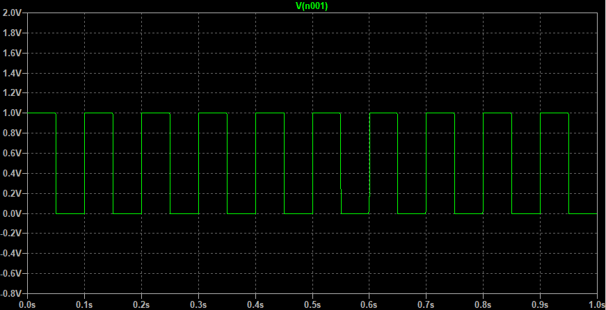
Subtraction circuit
Since subtraction is not positive or negative, we list it separately .
Subtraction is often used to output differential signals .
Its circuit is generally as follows :

among V_3 It's a sine wave :
V_4 For DC power supply 1V.
At the same time, the following conditions are also met :
- Deficiency :
V i n + = V i n − = V G N D Vin_+ = Vin_- = V_{GND} Vin+=Vin−=VGND
- Virtual break :
I i n + = I i n − = 0 Iin_+ = Iin_- = 0 Iin+=Iin−=0
among V_+ The calculation method of is as follows :
V + = R 4 R 1 + R 4 ∗ V i n + V_+ = \frac{R_4}{R_1+R_4} * Vin_+ V+=R1+R4R4∗Vin+
For the negative input, use KCL The analysis is as follows :
V i n − V G N D R 2 = V G N D − V o u t R 3 \frac{Vin_- V_{GND}}{R_2} = \frac{ V_{GND} - V_{out}}{R_3} R2Vin−VGND=R3VGND−Vout
take V i n + = V i n − = V G N D Vin_+ = Vin_- = V_{GND} Vin+=Vin−=VGND Brought in :
V o u t = V i n + R 4 R 1 + R 4 ( 1 + R 3 R 2 ) − V i n − ( R 3 R 2 ) V_{out} = Vin_+ \frac{R_4}{R_1+R_4}(1+\frac{R_3}{R_2}) - Vin_-(\frac{R_3}{R_2}) Vout=Vin+R1+R4R4(1+R2R3)−Vin−(R2R3)
When R 3 = R 4 And R 1 = R 2 R_3 = R_4 And R_1 =R_2 R3=R4 And R1=R2 When conditions are met
Simplify :
V o u t = R 3 R 2 ( V i n + − V i n − ) V_{out} = \frac{R_3}{R_2} ( Vin_+ - Vin_-) Vout=R2R3(Vin+−Vin−)
Meet the subtraction circuit .
The final simulation results are as follows :

among V(gnd) by V+ voltage ,V(n001) by V3 The signal ,Vout Such as the label in the simulation .
边栏推荐
- The number of digits of power and factorial
- MySQL paging
- What is cloud native? Why is cloud native technology so popular?
- Why can't memset initialize array elements to 1?
- 网络爬虫之短信验证
- 在线客服聊天系统源码_美观强大golang内核开发_二进制运行傻瓜式安装_附搭建教程
- ctfshow ThinkPHP专题 1
- This should be postman, the most complete interface testing tool in the whole network
- Installing MySQL under Linux
- Leetcode 257. all paths of binary tree
猜你喜欢

Fiddler packet capture tool summary

只会“点点点”,凭什么让开发看得起你?

How to choose sentinel vs. hystrix current limiting?

【C】 Understanding C language variable scope and life cycle from memory

视频回放 | 如何成为一名优秀的地学和生态学领域的国际期刊审稿人?

Depth first search and breadth first search of Graphs

JPS has no namenode and datanode reasons

selenium3自动化测试(这一篇就够了)——自学篇

tcp 服务端接收数据处理思路梳理,以及select: Invalid argument报错 笔记

JMeter interface test steps - Installation Tutorial - script recording - concurrent test
随机推荐
tcp 服务端接收数据处理思路梳理,以及select: Invalid argument报错 笔记
Self taught software testing talent -- not covered
Depth first search and breadth first search of Graphs
运算放大器 —— 快速复苏笔记[贰](应用篇)
The number of digits of power and factorial
【10】 Teamwork and cross team collaboration
The difference between YPbPr and YCbCr
Blue Bridge Cup provincial match training camp - Calculation of date
Semaphore details
如何从功能测试到自动化测试?
JMeter接口测试步骤-安装教程-脚本录制-并发测试
使用Prometheus+Grafana实时监控服务器性能
Best practice | using Tencent cloud AI character recognition to realize enterprise qualification certificate recognition
How to access the code of online customer service system to your website
Installing MySQL under Linux
Yum installation prompt to protect multi library version
强引用、软引用、弱引用、虚引用有什么区别?
About [software testing - interview skills and precautions for automated testing] - talk freely
Simply use MySQL index
Use Modelsim to independently simulate Altera and Xilinx IP cores