当前位置:网站首页>IR drop, EM, noise and antenna
IR drop, EM, noise and antenna
2022-07-23 17:07:00 【Luca cat】
List of articles
1. IR Drop
IR Drop It refers to a phenomenon of voltage drop and rise on the power supply and ground network in an integrated circuit . Due to the continuous evolution of Technology , The width of metal interconnects is getting narrower , The resistance value is increasing , The supply voltage is getting smaller and smaller ,IR Drop The effect of is becoming more and more obvious . therefore , Now the chips are finally IR Drop As a chip signoff A necessary step of . The tool uses Redhawk.
1.1 IR Drop The classification of
IR Drop There are two main types . One is Static IR Drop, The other is Dynamic IR Drop.
static state IR Drop The main reason is the partial voltage of the metal connection of the power network , Caused by the resistance partial voltage of the metal wiring itself . The static voltage is mainly related to the structure and detailed wiring of the power network .
static state IR Drop Mainly consider the resistance effect , Analyze the effect of resistance .
dynamic IR Drop The cause is the voltage drop caused by current fluctuation when the power supply is switched , Occurs on the trigger edge of the clock , The clock edge jump causes a large number of transistor switches , Bring about the jump of combinational logic circuit , Make the chip generate a large current in a short time .
The more transistors the switch has , The easier it is to trigger dynamics IR Drop The phenomenon .
1. 2 IR drop Influence
Performance degradation, When the voltage drops ,gate The switching speed of becomes slow , Performance degradation . So for high-performance design ,IR Drop It needs to be controlled within a very small range .Lead to setup and hold Violation, If power network Not good enough ,IR drop Especially large in a local area ( Especially dynamic IR Drop), Which leads to STA Stage signoff Of timing Not consistent with the actual situation .
setup The violation of can raise the frequency by raising the voltage , But the power consumption goes up , And if dynamic IR drop Not enough robust, By raising the voltage ,setup There is also limited room for improvement .
Once it appears hold Violation , Then the chip will not work properly . Therefore, in advanced technology ,IR Drop The impact is particularly great , It needs to attract your great attention .
1.3 improve IR Drop Methods
Improve PG density , increase power switch cell Number , enhance PG Strength ofInsert enough decap cell( Including decoupling capacitor )Stagger the flipped registers row put
2. EM
EM( Electromigration ): Metal as interconnection , When the current is too high , Electrons collide with atoms inside the metal , Cause metal to heat , The resistance increases , When a large number of collisions occur in a short time , Metal atoms will flow in the direction of electrons , This phenomenon is called Electromigration .
Interconnection :IC The internal use of metal film to conduct the working current is called interconnection .
2.1 EM influence
- Electromigration will make IC There is a short circuit or open circuit in the interconnection line , cause IC invalid .
- Increase the grid resistance of the power supply , Affect circuit timing
2.2 improve EM Method
- You need to double the width of the line
- increase via The number of
3. Noise Violation
noise Also known as crosstalk( crosstalk ), Mainly refers to Process metal layer line narrowed , After the spacing becomes smaller , As a result, the coupling capacitance between lines increases , The grounding capacitance becomes smaller . and Noise The size of is directly proportional to the coupling capacitance , It is inversely proportional to the grounding capacitance . So lead to Noise The impact of .
noise The impact of is mainly divided into two categories : Signal delay and burr
Based on the analysis of noise when , Will produce noise The network of signal sources is called infringement net, Networks that are subject to crosstalk are called victims net. When the signal of network infringement is 0 and 1 When the level changes between , The affected network will generate corresponding crosstalk noise .
3.1 Repair noise violation Methods
Enhance victimization net The driving power of,upsize driverTo the victim net Add buffer, insert buffer It's back-end repair violation Universal means . It also deals with noise It is a very effective repair technology . By inserting buffer Breaking the long line can effectively reduce the victims net Coupling capacitance on , To reduce noise Influence .- Reduce the length of parallel routes , change net Routing
- Put two net Increase the spacing between or shield wire shield To protect victims net
- Reduce the driving power of infringing network
4. antenna violation
antenna violation( Antenna effect ): In the process of chip production , Exposed metal wires and other conductors , Like antennas Collect charge Cause the potential to rise . When there is enough charge, it will discharge , Probably breakdown MOS The grid of the tube , Disable the circuit , Namely Antenna effect .
With the development of Technology , The size of the grid is getting smaller and smaller , There are more and more layers of metal , The more likely the antenna effect is .
4.1 Elimination method of antenna effect
The method to solve the antenna effect can be divided into jumper sending ( Upper jumper and lower jumper )、 Plug in the diode 、 insert buffer.
1. Upward jumper method 

2. Downward jumper method
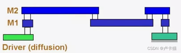
This method solves the antenna effect by changing the level of metal wiring , But at the same time, through holes are added , Because the resistance of the through hole will directly affect the timing and crosstalk of the chip , Therefore, strictly control the change of wiring level and the number of through holes .
These two methods , Among them, the upward jumper method is the most commonly used , Only when the antenna effect appears on the top metal layer , Just consider jumping down . But the effect is not obvious , You can directly use another method below , insert buffer Cut off the long line .
3. Insert the reverse diode
Insert a grounded diode into the metal connection line , When the charge accumulates to a certain extent , It will form a path to the ground , But inserting a diode will increase the chip area , It is not suitable to adopt .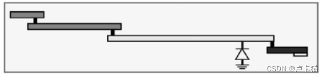
4. insert buffer
Insert buffer Cut off the long line , Solve the antenna effect .
5.sizeup cell
Increase the area of the grid to reduce the antenna effect
6. add to dummy load load
The essence is to increase gate To alleviate the antenna effect . Generally used for smaller violation The situation of .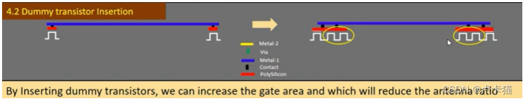
边栏推荐
- 目前有哪些年利率6%左右的保本理财产品?
- What are the principal guaranteed financial products with an annual interest rate of about 6%?
- 腾讯撕开中国NFT的“遮羞布”
- Advanced authentication of uni app [Day12]
- uni-app进阶之认证【day12】
- Notes on Microcomputer Principle and technical interface
- Leetcode-168.excel table column name
- Squeeze and incentive networks
- Compose Canvas饼图效果绘制
- MATLAB基础
猜你喜欢

软件配置 | Anaconda下载、安装及环境配置和卸载
虾皮二面:JVM内存布局你知道的都说一下?

通过SSH方式访问内网RDS+mysql

Direct exchange

AutoCAD基本操作

简单了解首个 EVM 等效的 zkEVM Polygon 为何全力押注

TOPSIS法(MATLAB)
Priyanka Sharma, general manager of CNCF Foundation: read CNCF operation mechanism

Bag of tricks for image classification "with convolutional neural networks"

Lake Shore—EMPX-H2 型低温探针台
随机推荐
PWN entry (3) heap
【Flutter -- 布局】线性布局(Row 和 Column)
Function secondary development / plug-in development of JMeter (detailed version)
Fundamentals of C language -- 2-6 pointers, arrays and sizeof operators
通用分页功能
通用分页实现
AXI interconnect IP核的说明及用法
Sprintf and cv:: puttext
AutoCAD基本操作
Summary of after class homework of Microcomputer Principle and technical interface
七月集训(第23天) —— 字典树
Is it safe for online account managers to open accounts when choosing securities companies in flush
Solve data functions should return an object (property "visible" must be accessed with "$data.visible")
Add dependent jar packages to the project in the idea
sprintf和cv::putText
[30. N-queen problem]
使用“soup.h1.text”爬虫提取标题会多一个\
本周投融报:Web3游戏熊市吸金
PIP reports an error could not find a version that satisfies the... No matching distribution
uni-app进阶之认证【day12】