当前位置:网站首页>PCB layout must know: teach you to correctly lay out the circuit board of the op amp
PCB layout must know: teach you to correctly lay out the circuit board of the op amp
2022-08-05 10:18:00 【Ji Ke Lao Bai】
In the circuit design process, application engineers often overlook the layout of the printed circuit board (PCB).The problem often encountered is that the schematic of the circuit is correct, but it doesn't work, or just runs at low performance.
In this article, a great engineer will show you how to properly lay out an op amp's circuit board to ensure its functionality, performance, and robustness.
Incident Replay
Engineers and their intern designed with an OPA191 op amp in a non-inverting configuration with a gain of 2V/V, a load of 10k, and a supply voltage of +/-15V.Figure 1 shows a schematic of the design.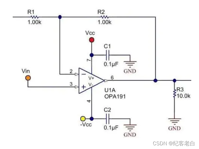
Figure 1 OPA191 schematic in non-inverting configuration
The engineer assigns the intern to lay out the board for this design and gives him general guidance on PCB layout (ie, keep the board trace paths as short as possible, while keeping the components close together to reduce the size of the boardspace) and let him design it himself.
How difficult is the design process?It's really just a few resistors and capacitors, isn't it?
Figure 2 shows the layout of the interns' first attempt at designing.The red line is the path for the top layer of the board, while the blue line is the path for the bottom layer.![[image]](/img/52/2241495f834f3926c0a37c377efd7c.png)
Figure 2 First Layout Attempt Scheme
Realized CircuitThe board layout wasn't as intuitive as I thought it would be, and the engineer felt that there should be some more detailed instructions for the interns.The intern followed his advice exactly when designing, shortening the traces and placing the components closely together.But this layout can be further improved to reduce board parasitic impedance and optimize its performance.
The first improvement they made was to move resistors R1 and R2 next to the inverting pin (pin 2) of the OPA191; this helped reduce stray capacitance on the inverting pin.
The inverting pin of an op amp is a high impedance node and therefore has high sensitivity.Longer trace paths can act as wires, allowing high frequency noise to couple into the signal chain.PCB capacitance on the inverting pin can cause stability problems.Therefore, the contact on the inverting pin should be as small as possible.
Moving R1 and R2 next to pin 2 allows the load resistor R3 to be rotated 180 degrees, which brings decoupling capacitor C1 closer to the positive supply pin (pin 7) of the OPA191.It is extremely important to place the decoupling capacitors as close as possible to the supply pins.Longer trace paths between the decoupling capacitors and the power supply pins increase the inductance of the supply pins, which reduces performance.
Another improvement they made is the second decoupling capacitor C2.The via connection of VCC to C2 should not be placed between the capacitor and the power supply pins, but should be routed where the supply voltage must pass through the capacitors to the power supply pins of the device.
Figure 3 shows how to move each part and vias to improve the layout.![[image]](/img/6c/e42ad51abf393da7c2e81993b80e44.png)
Figure 3 The position of each component to improve the layout
You can addWide trace paths to reduce inductance, which is equivalent to the size of the pads that the trace paths connect to.It can also flood the ground planes on the top and bottom layers of the board, creating a solid, low-impedance path for return current.Figure 4 shows the final layout.![[image]](/img/c5/545fc7509306be4b4c1b3a39757a1c.png)
Figure 4 Final layout----
边栏推荐
猜你喜欢

【MindSpore Easy-Diantong Robot-01】You may have seen many knowledge quiz robots, but this one is a bit different

FPGA:开发环境Vivado的使用

气象数据数据处理实例——matlab字符串切割匹配与R语言日期匹配(数据拼接)

一文道清什么是SPL

项目成本控制如何帮助项目成功?

如何选币与确定对应策略研究
The JVM collection that Alibaba's top architects have summarized for many years, where can't I check it!

七夕浪漫约会不加班,RPA机器人帮你搞定工作

Introduction to SD NAND Flash!
linux下oracle常见操作以及日常积累知识点(函数、定时任务)
随机推荐
The difference between find, matches, lookingAt matching strings in matcher
七夕浪漫约会不加班,RPA机器人帮你搞定工作
How does the official account operate and maintain?Public account operation and maintenance professional team
数据中台建设(十):数据安全管理
Wei Dongshan Digital Photo Frame Project Learning (6) Transplantation of tslib
High-quality DeFi application building guide to help developers enjoy DeFi Summer
电气工程的标准是什么
华为轻量级神经网络架构GhostNet再升级,GPU上大显身手的G-GhostNet(IJCV22)
Voice-based social software development - making the most of its value
高质量 DeFi 应用构建指南,助力开发者玩转 DeFi Summer
ffmpeg drawtext add text watermark
Advanced usage of C language
PCB布局必知必会:教你正确地布设运算放大器的电路板
阿里全新推出:微服务突击手册,把所有操作都写出来了PDF
IO stream articles -- based on io stream to realize folder copy (copy subfolders and files in subfolders) full of dry goods
E-sports, convenience, efficiency, security, key words for OriginOS functions
【综合类型第 35 篇】程序员的七夕浪漫时刻
Oracle temporary table space role
Go compilation principle series 6 (type checking)
数分面试(一)----与业务相关