当前位置:网站首页>FPGA - 7 Series FPGA selectio -07- iserdese2 of advanced logic resources
FPGA - 7 Series FPGA selectio -07- iserdese2 of advanced logic resources
2022-06-28 06:21:00 【Vuko-wxh】
Preface
Excerpts from this article UG471 Chapter three of , Organize and translate , Used to introduce SelectIO Resource internal ISERDESE2 resources . Input serial parallel converter (ISERDESE2) And output parallel serial converter (OSERDESE2) Support very fast I/O Data rate , And allow the internal logic to run at a lower speed 8 times Than I/O.
Input serial parallel logic resources (ISERDESE2) brief introduction
7 series FPGA Medium ISERDESE2 It is a special serial parallel converter , It has specific clock and logic functions , It aims to promote the implementation of high-speed source synchronization applications . ISERDESE2 To avoid the in FPGA Additional timing complexity encountered when designing deserializers in the architecture .
ISERDESE2 Features include :
Special deserializer / Serial to parallel converter
ISERDESE2 The deserializer can realize high-speed data transmission , There is no need to FPGA Schema matching input data frequency . The converter supports single data rate (SDR) And dual data rate (DDR) Pattern . stay SDR In mode , The serial parallel converter creates a 2 position 、3 position 、4 position 、5 position 、6 position 、7 Bit or 8 Bit wide parallel word . stay DDR In mode , The serial parallel converter is using a ISERDESE2 Created on 4、6、8 Bit width parallel word mode , Using two cascades ISERDESE2 Created on 10 Bit or 14 Bit width parallel word mode .
Bitslip Sub module
Bitslip Submodules allow designers to reorder into FPGA A sequence of parallel data streams of the architecture . This can be used to train source synchronization interfaces that contain training patterns .
Specifically support strobe based memory interfaces
ISERDESE2 Including dedicated circuits ( Include OCLK Input pin ) To be completely in ISERDESE2 Process gating in the module to FPGA Clock domain crossover . This allows for higher performance and simplified implementation .
Dedicated support for network interfaces
Dedicated support DDR3 Interface
Dedicated support QDR Interface
Specifically support asynchronous interfaces
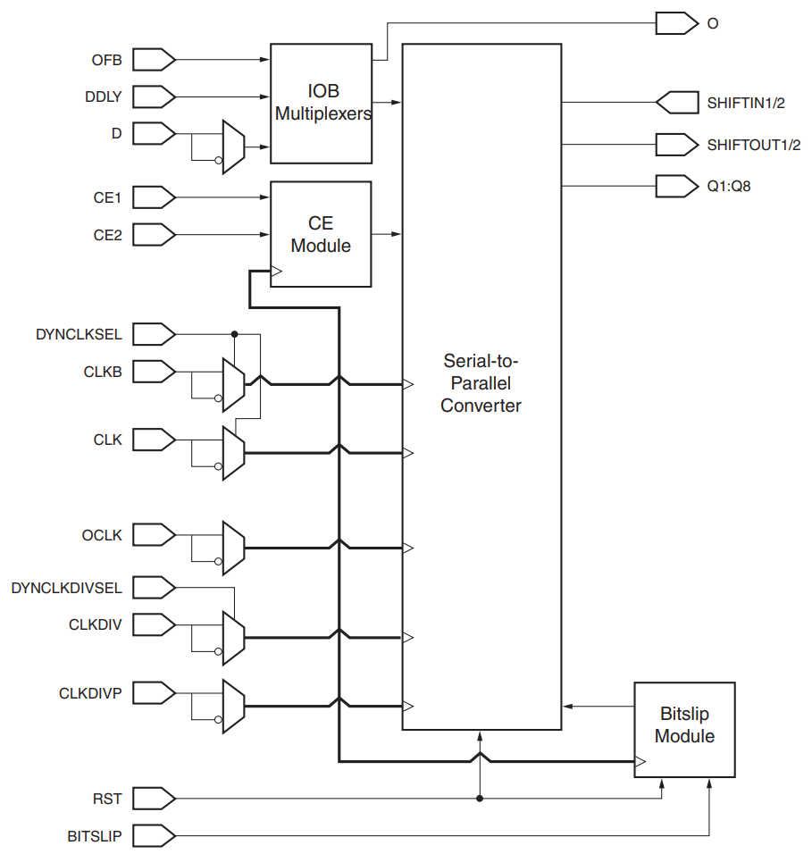
The image below shows ISERDESE2 Diagram of , All the main components and functions of the module are highlighted , Including optional inverter .
ISERDESE2 The original language (ISERDESE2)
7 In a series of devices ISERDESE2 The primitive structure is shown in the following figure .
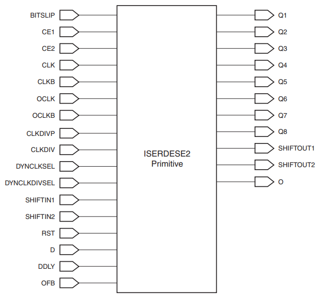
The following table lists them ISERDESE2 Available ports in primitives .
| Port Name | Type | Width | Description |
|---|---|---|---|
| Q1 – Q8 | Output | 1 (each) | Deposited output . |
| O | Output | 1 | Combined output . |
| SHIFTOUT1 | Output | 1 | Expand the data width . Connect to and from IOB Of SHIFTIN1. |
| SHIFTOUT2 | Output | 1 | Expand the data width . Connect to and from IOB Of SHIFTIN2. |
| D | Input | 1 | come from IOB Serial input data of . |
| DDLY | Input | 1 | come from IDELAYE2 Serial input data of . |
| CLK | Input | 1 | High speed clock input . Clock serial input data stream . |
| CLKB | Input | 1 | The second high-speed clock input is only applicable to MEMORY_QDR Pattern . Except in MEMORY_QDR In mode , Otherwise, it is always connected to the inverting CLK. |
| CE1, CE2 | Input | 1 (each) | Clock enable input . |
| RST | Input | 1 | High level active reset . |
| CLKDIV | Input | 1 | Frequency division clock input . Clock delay element 、 Deserialized data 、Bitslip Module and CE unit . |
| CLKDIVP | Input | 1 | Only through MIG Tool support . stay MEMORY_DDR3 In mode by PHASER_IN frequency division CLK Provide . All other modes are grounded . |
| OCLK | Input | 1 | High speed clock inputs for memory applications . ( At this time, the clock resource and OSERDESE2 CLK Pin sharing .) |
| OCLKB | Input | 1 | Inverse high-speed clock input . ( At this time, the clock resource and OSERDESE2 CLKB Pin sharing .) |
| BITSLIP | Input | 1 | call Bitslip operation . |
| SHIFTIN1 | Input | 1 | Carry the input of data width extension . Connect to the main IOB Of SHIFTOUT1. |
| SHIFTIN2 | Input | 1 | Carry the input of data width extension . Connect to the main IOB Of SHIFTOUT2. |
| OFB | Input | 1 | come from OLOGICE2 or OLOGICE3 and OSERDESE2 The feedback path of the output . |
| DYNCLKDIVSEL | Input | 1 | Dynamic selection CLKDIV reverse . |
| DYNCLKSEL | Input | 1 | Dynamic selection CLK and CLKB reverse . |
ISERDESE2 port
Deposit output – Q1 to Q8
Output port Q1 to Q8 yes ISERDESE2 Register output of the module . One ISERDESE2 The module can support up to 8 position ( namely 1:8 Deserialization ). Only in DDR Mode can support greater than 8 position ( most 14 position ) The bit width of . The first data bit received appears in the highest order Q On the output .
OSERDESE2 The input bit order is the same as ISERDESE2 The bit order of the module output is reversed , As shown in the figure below .

for example , word FEDCBA The least significant bit of A Put in OSERDESE2 Of D1 Input end , But the same bit A Appear in the Q8 The output of ISERDESE2 In block . let me put it another way ,D1 yes OSERDESE2 Minimum valid input for , and Q8 yes ISERDESE2 Minimum valid output of the module . When using width expansion , transmitter OSERDESE2 Of D1 Is the least valid input , And the receiver ISERDESE2 Modular Q8 Is the least significant output .
Combined output – O
Combined output port (O) yes ISERDESE2 Unregistered output of the module . This output can come directly from the data input (D), It can also come from IDELAYE2 Data input of (DDLY).
Bitslip operation - BITSLIP
BITSLIP Pin is asserting ( High active ) Execute with CLKDIV synchronous Bitslip operation . And then , stay Q1 To Q8 The data seen on the output port will move , Just like in barrel shifter operation , Every time you call Bitslip Move a position when (DDR Operation and SDR Different ).
Clock enable input - CE1 and CE2
Every ISERDESE2 Each module contains an input clock enable module .
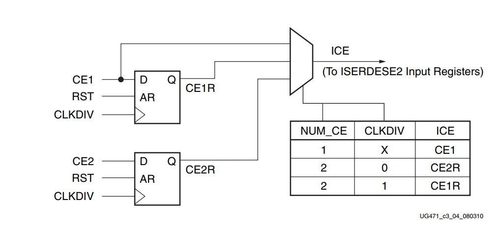
When NUM_CE = 1 when , Don't use CE2 Input ,CE1 Input is directly connected to ISERDESE2 Valid high clock enable of the input register in . When NUM_CE = 2 when , Use at the same time CE1 and CE2 Input ,CE1 Enable ISERDESE2 Of 1/2 individual CLKDIV cycle ,CE2 Enable ISERDESE2 Another ½. The internal clock enable signal shown in the figure above ICE come from CE1 and CE2 Input .
The clock enable module is used as 2:1 Serial to parallel converter , from CLKDIV Provide clock . When ISERDESE2 Configure to DDR Mode of 1:4 When deserializing , The bidirectional memory interface requires a clock enable module . When the attribute NUM_CE = 2 when , The clock enable module is enabled and CE1 and CE2 Ports are available . When NUM_CE = 1 when , Only CE1 Can be used as a regular clock enable .
High speed clock input - CLK
High speed clock input (CLK) Used to provide a clock for the input serial data stream .
High speed clock input - CLKB
High speed auxiliary clock input (CLKB) Used to provide a clock for the input serial data stream . stay MEMORY_QDR In any mode other than , take CLKB Connect to CLK Inverse version of . stay MEMORY_QDR In mode ,CLKB It shall be connected to a unique phase shift clock .
Frequency division clock input - CLKDIV
Frequency division clock input (CLKDIV) Usually CLK Frequency division version of ( Depending on the width of the de concatenation implemented ). It drives the serial parallel converter 、Bitslip Module and CE Module output .
come from IOB Serial input data of - D
Serial input data port (D) yes ISERDESE2 Serial ( High speed ) Data input port . This port is only connected to 7 series FPGA IOB Resources are used together .
IDELAYE2 Serial input data of - DDLY
Serial input data port (DDLY) yes ISERDESE2 Serial ( High speed ) Data input port . This port is only connected to 7 series FPGA IDELAYE2 Resources are used together .
come from OSERDESE2 Serial input data of - OFB
Serial input data port (OFB) yes ISERDESE2 Serial ( High speed ) Data input port . This port is only connected to 7 series FPGA OSERDSE2 port OFB In combination with .
High speed clock based on strobe memory interface and oversampling mode - OCLK
OCLK Clock input synchronization is based on data transmission in strobe memory interface . OCLK The clock is only on INTERFACE_TYPE Set to NETWORKING Do not use .
OCLK The clock input can be used to transfer strobe based memory data to the free running clock domain . OCLK Is a free running FPGA The clock , Its frequency is similar to CLK The strobe pulses on the input are the same . from CLK To OCLK The domain transmission of is shown in the figure 3-5 As shown in the block diagram . The timing of domain transmission is determined by the user by adjusting the strobe signal to CLK Enter the delay to set ( for example , Use IDELAY). Memory interface generator (MIG) Is given in MEMORY_DDR3 and MEMORY_QDR Example of mode setting the transmission timing of this domain . When INTERFACE_TYPE by NETWORKING when , This port is not used .
Reset input - RST
Setting time , Resetting the input will cause CLK and CLKDIV The output of most data triggers in the domain is asynchronously driven to low level . The exception is the first four triggers in the input structure , The reset value can be selected by attributes on the component . When and CLKDIV When synchronizing cancel assertion , The internal logic will re - time this cancellation assertion to CLK The first rising edge of . therefore , Each in a multi bit input structure ISERDESE2 Shall be driven by the same reset signal , And CLKDIV Synchronous set and low , To make sure that all ISERDESE2 Element synchronization exit reset . Only if known CLK and CLKDIV Stable and existing , The set reset signal should be cancelled , And there should be at least two CLKDIV Pulse width . After the reset is invalid , Output in two CLKDIV Only after the cycle .
ISERDESE2 attribute
The following table summarizes all applicable ISERDESE2 attribute , A detailed description of each attribute is shown in the following table .
| Attribute Name | Description | Value | Default Value |
|---|---|---|---|
| DATA_RATE | Allows incoming data streams to be treated as SDR or DDR Data processing . | String: SDR or DDR | DDR |
| DATA_WIDTH | Define the width of the serial parallel converter . Legal value depends on DATA_RATE attribute (SDR or DDR). | Integer: 2, 3, 4, 5, 6, 7, 8, 10 or 14. DATA_RATE = DDR, value is limited to 4, 6, 8, 10, or 14. DATA_RATE = SDR, value is limited to 2, 3, 4, 5, 6, 7, or 8. | 4 |
| DYN_CLKDIV_INV_EN | When TRUE When enabled DYNCLKDIVSEL reverse , And disable CLKDIV On the pin HDL reverse . | Boolean: TRUE or FALSE | FALSE |
| DYN_CLK_INV_EN | When TRUE When enabled DYNCLKSEL Reverse and disable CLK and CLKB On the pin HDL reverse . | Boolean: TRUE or FALSE | FALSE |
| INTERFACE_TYPE | choice ISERDESE2 Usage mode . | String: MEMORY, MEMORY_DDR3, MEMORY_QDR, OVERSAMPLE, or NETWORKING | MEMORY |
| NUM_CE | Define the number of clock enablers . | Integer: 1 or 2 | 2 |
| OFB_USED | Enable from OLOGICE2/3、 OSERDESE2 OFB Pin to ISERDESE2 OFB The path of the pin . Ban D Input pin . | Boolean: TRUE or FALSE | FALSE |
| SERDES_MODE | Define when using width extension ISERDESE2 Is the module a master module or a slave module . | String: MASTER or SLAVE | MASTER |
| INIT_Q1 | Set the initial value of the first sample register . | Binary: 0 or 1 | 0 |
| INIT_Q2 | Set the initial value of the second sample register . | Binary: 0 or 1 | 0 |
| INIT_Q3 | Set the initial value of the third sample register . | Binary: 0 or 1 | 0 |
| INIT_Q4 | Set the initial value of the fourth sample register . | Binary: 0 or 1 | 0 |
| SRVAL_Q1 | Set the value of the first sample register after reset . | Binary: 0 or 1 | 1 |
| SRVAL_Q2 | Set the value of the second sampling register after reset . | Binary: 0 or 1 | 1 |
| SRVAL_Q3 | Set the value of the third sampling register after reset . | Binary: 0 or 1 | 1 |
| SRVAL_Q4 | Set the value of the fourth sampling register after reset . | Binary: 0 or 1 | 1 |
| IOBDELAY | Set whether the input delay applies to deposit and / Or non deposit output . | NONE, IBUF, IFD, or BOTH | NONE |
DATA_RATE attribute
DATA_RATE Property defines the incoming data flow as a single data rate (SDR) Or dual data rate (DDR) Handle . The allowed values for this attribute are SDR and DDR. The default value is DDR.
DATA_WIDTH attribute
DATA_WIDTH Property defines the parallel data output width of the serial to parallel converter . The possible values for this attribute depend on INTERFACE_TYPE and DATA_RATE attribute . About supported data widths , See the table below .

When DATA_WIDTH Set to greater than 8 The width of , a pair ISERDESE2 Must be configured as master-slave configuration . Width expansion is not allowed in memory mode .
INTERFACE_TYPE attribute
INTERFACE_TYPE Attribute determination ISERDESE2 Whether to configure in memory mode or network mode . The allowed values for this attribute are MEMORY、MEMORY_DDR3、MEMORY_QDR、OVERSAMPLE or NETWORKING. The default mode is memory .
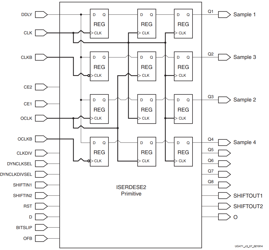
chart 3-5 It shows that MEMORY Mode of ISERDESE2 Internal connection .

NUM_CE attribute
NUM_CE Property defines the number of clock enablers used (CE1 and CE2). The possible value is 1 and 2( The default value is = 2).
SERDES_MODE attribute
SERDES_MODE Property defines when using width extension ISERDESE2 Is the module a master module or a slave module . The possible value is MASTER and SLAVE. The default value is MASTER.
ISERDESE2 Clock method
NETWORKING Interface type
CLK and CLKDIV The phase relation of is very important in the process of serial parallel conversion . CLK and CLKDIV( Ideally ) Phase alignment within tolerance .FPGA There are a variety of clock arrangements to help design to meet CLK and CLKDIV Phase relationship requirements for .
CLK and CLKDIV Input must be nominal phase aligned . for example , If the designer is ISERDESE2 The input end will be shown in the figure below CLK and CLKDIV Reverse phase , So although the clock arrangement is allowed BUFIO/BUFR To configure , But the clock will still be out of phase . This also prohibits the use of DYNCLKINVSEL and DYNCLKDIVINVSEL.

Use network interface type ISERDESE2 The only valid clock arrangement for the module is :
- from BUFIO Driven CLK, from BUFR Driven CLKDIV.
- CLK from MMCM or PLL drive ,CLKDIV By the same MMCM or PLL Of CLKOUT[0:6] drive .
When using MMCM drive ISERDESE2 Of CLK and CLKDIV when , Cannot be mixed into ISERDESE2 Type of buffer provided . for example , If CLK from BUFG drive , be CLKDIV It must also be BUFG drive . perhaps ,MMCM Can pass BUFIO and BUFR drive ISERDESE2.
Memory interface type
Use memory interface type ISERDESE2 The only valid clock schedule for the module is :
- from BUFIO Driven CLK、 from BUFIO Driven OCLK And from BUFR Driven CLKDIV.
- CLK from MMCM or PLL drive ,OCLK from MMCM or PLL drive ,CLKDIV By the same MMCM or PLL Of CLKOUT[0:6] drive .
- BUFG Driven CLK、BUFG Driven OCLK、 Different BUFG Driven CLKDIV.
OCLK and CLKDIV Input must be nominal phase aligned . expect CLK and OCLK There is no phase relationship . Calibration must be performed to achieve from CLK To OCLK Reliable data transmission of domain . High speed clock based on strobe memory interface and oversampling mode - OCLK Provide information about in CLK and OCLK More information about transferring data between .
MEMORY_QDR Interface type
because QDR Memory requirements ,MEMORY_QDR The mode has a complex clock structure . Use only MIG Tool INTERFACE_TYPE Property settings .
OVERSAMPLE Interface type
OVERSAMPLE Mode is used to collect two phases DDR data . chart 3-7 Shows ISERDESE2 A more detailed logical representation of , And how to CLK and OCLK The rising and falling edges of capture data . Pictured 3-7 Shown ,CLK and OCLK There must be 90° Offset phase relation , Because the data is CLK and OCLK Are captured , But in CLK Field from ISERDESE2 Clock output . Do not use in this mode CLKDIV. OVERSAMPLE The only valid clock schedule for an interface type is :
- CLK and CLKB from BUFIO drive . OCLK and OCLKB By phase shift 90° Of BUFIO drive . Two BUFIO By a single MMCM drive .
- CLK and CLKB from BUFG drive . OCLK and OCLKB By phase shift 90° Of BUFG drive . BUFG By a single MMCM drive . In any case , The valid clock is :
- CLK:0°
- OCLK:90°
- CLKB:180°
- OCLKB:270°
MEMORY_DDR3 Interface type
because DDR3 Memory requirements ,MEMORY_DDR3 The mode has a complex clock structure . Use only MIG Tool INTERFACE_TYPE Property settings .
ISERDESE2 Width expansion
Two ISERDESE2 Modules can be used to build larger than 1:8 The serial to parallel converter . At every I/O There are two in each block ISERDESE2 modular ; A master from . By putting the Lord ISERDESE2 Of SHIFTOUT The port is connected to the slave ISERDESE2 Of SHIFTIN port , The serial to parallel converter can be extended to up to 1:10 and 1:14( Limited to DDR Pattern ).
The following figure shows the use of master-slave ISERDESE2 Cascading of modules DDR Block diagram of serial parallel converter . stay 1:10 SERDES Under the circumstances , From port Q3-Q4 The last two bits for the parallel interface . For differential inputs , Lord ISERDESE2 Must be at the positive pole of the differential input pair (_P Pin ) Side . When the input is not differential , And from the ISERDESE2 The associated input buffer is not available , Therefore, cascading... Cannot be used .

A guide to expanding the bit width of a serial parallel converter
Two ISERDESE2 Modules must be adjacent master-slave pairs . Two ISERDESE2 All modules must be in NETWORKING Pattern , Because the width expands in MEMORY Not available in mode .
Will the Lord ISERDESE2 Of SERDES_MODE Property is set to MASTER, Subordinate ISERDESE2 Set to SLAVE.
Users have to put SLAVE Of SHIFTIN Port to MASTER Of SHIFTOUT port .
SLAVE The use of port Q3 To Q8 As the output .
DATA_WIDTH This applies to MASTER and SLAVE.
ISERDESE2 Delay
When ISERDESE2 The interface type is MEMORY when , adopt OCLK The delay of the phase is one CLKDIV cycle . However , adopt ISERDESE2 The total delay of depends on CLK and OCLK Phase relationship between clock inputs . When ISERDESE2 The interface type is NETWORKING when , The delay is two CLKDIV cycle .
Additional in network mode CLKDIV Delay cycle ( Compared with memory mode ) Is due to Bitslip Sub module .MEMORY_QDR and MEMORY_DDR3 The delay in is two CLKDIV cycle .
Dynamic clock reversal
Dynamic clock reverse pin DYNCLKSEL and DYNCLKDIVSEL Respectively with DYN_CLK_SEL_EN and DYN_CLKDIV_SEL_EN When used together , It allows users to dynamically switch the polarity of their clock sources . This operation results in entry ISERDESE2 Clock asynchronous switching , And may lead to ISERDESE2 Generate wrong data , until ISERDESE2 Reset . This operation can only be performed in MEMORY_QDR and MEMORY_DDR3 Support for .
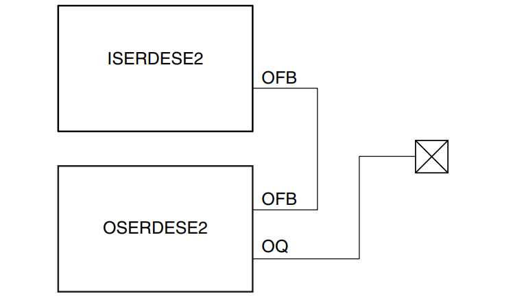
ISERDESE2 come from OSERDESE2 Feedback
ISERDESE2 and OSERDESE2 Medium OFB The port can be used to connect OSERDESE2 The data transmitted on the is fed back to ISERDESE2( chart 3-9). When the attribute OFB_USED = TRUE Enable this feature when . OSERDESE2 and ISERDESE2 Must have the same DATA_RATE and DATA_WIDTH Set up , So that feedback can provide correct data . Use only in width extended mode ISERDESE2 and OSERDESE2 when , Will the Lord OSERDESE2 Connect to the main ISERDESE2.
By using ISERDESE2 As a feedback port , It cannot be used as input to external data .
stay ISERDESE2 Use in D and DDLY
D and DDLY The pin is ISERDESE2 Special input for .D Input is directly connected to IOB. DDLY The pin is directly connected to IDELAYE2. This allows the user to check on the (Q1-Q8) Or combined path (O) The input of the output has a delayed or non delayed version . attribute IOBDELAY Be sure to apply to ISERDESE2 The input of .
The following table shows D and DDLY When both are connected IOBDELAY Result of each setting of the value . When D and DDLY All connected to ISERDESE2 when , relation IOBDELAY On block IOBDELAY Property value .
| IOBDELAY Value | Combinatorial Output (O) | Registered Output (Q1-Q8) |
|---|---|---|
| NONE | D | D |
| IBUF | DDLY | D |
| IFD | D | DDLY |
| BOTH | DDLY | DDLY |
ISERDESE2 Time series model and parameters
The following table describes 7 series FPGA In the data book ISERDESE2 Functions and control signals of switch characteristics .

Timing characteristics
The image below shows ISERDESE2 Input data to ISERDESE2 Sequence diagram .
Different modes (SDR/DDR) The name of the timing parameter will be different . however , When the bus input width is different , The name will not change , Including when two ISERDESE2 Cascade together to form 10 Bit or 14 When a . stay DDR In mode , data input (D) At every CLK edge ( Rise and fall ) Switch .

Clock Events 1
In time TISCCK_CE, In the clock event 1 Before , The clock enable signal becomes an active high level and ISERDESE2 You can sample data .
Clock Events 2
In time TISDCK_D, In the clock event 2 Before , Input data pin (D) Becomes valid and samples along the next clock .
ISERDESE2 VHDL and Verilog Instantiation templates are available in Library guides for all primitives and submodules .
BITSLIP Sub module
7 All in the series ISERDESE2 Each block contains a Bitslip Sub module . This sub module is used for word alignment purposes in source synchronous network type applications .Bitslip Yes ISERDESE2 Reorder the parallel data in the module , Each combination of repeated serial patterns received by the deserializer is allowed to be presented to FPGA framework . This repeated serial mode is often referred to as the training mode ( Many network and telecommunications standards support training patterns ). In some interfaces , This may be a slow forwarding clock , It can be thought of as a repeating bit pattern .
Bitslip operation
By setting ISERDESE2 Modular Bitslip Pin , The incoming serial data stream is reordered on the parallel side . Repeat this operation , Until ISERDESE2 See the desired training mode in the output . The table in the following figure illustrates SDR and DDR In mode Bitslip The effect of the operation . ( Input ISERDESE2 Of the 8 Bit is the first bit received .) For illustrative purposes , Data width is 8. Bitslip Operation and CLKDIV Sync . stay SDR In mode , Every Bitslip Operation will shift the output mode one bit to the left . stay DDR In mode , Every Bitslip Operation will cause the output mode to shift one bit to the right , Shift left three places . In this example , At the eighth Bitslip In operation , The output mode returns to the initial mode . This assumes that the serial data is in the 8-bit repeat mode .
Although the repetition pattern seems to indicate that bit slip is a barrel shift operation , But that's not the case . The bit slip operation adds a bit to the input stream and loses the first bit in the input stream n position . This causes the operation of the repeating pattern to look like a barrel shifter operation .

Bitslip Sub module usage guide
stay NETWORKING In mode ,Bitslip Submodules are available . In all other modes , The module is not available .
To be called Bitslip operation ,BITSLIP The port must be in a CLKDIV High level is built in the cycle .
Bitslip Not in two consecutive CLKDIV Is asserted in a cycle ;Bitslip Must be in two Bitslip At least one between assertions CLKDIV Deasserting within a cycle .
stay SDR and DDR In mode , from ISERDESE2 Capture the bit slip input of the assertion to “ Positional slip ” ISERDESE2 Output Q1-Q8 By CLKDIV Sample to FPGA The total delay of logic time is two CLKDIV cycle . From an application point of view , One Bitslip The command must be for only one CLKDIV Cycle issue . After analyzing the received data code type, another Bitslip Before the command , User logic should be in SDR Wait for at least two... In mode CLKDIV Cycle or in DDR Wait for three... In mode CLKDIV cycle . If ISERDESE2 Reset ,Bitslip The logic will also reset and return to its initial state .
Bitslip Time series model and parameters
The following discussion is related to 1:4 DDR The configuration of the Bitslip Controller related timing model .
data (D) It's repetitive 4 Bit training mode ABCD. ABCD Can appear in four possible ways ISERDESE2 Parallel output of Q1-Q4 On :ABCD、BCDA、CDAB and DABC. Only one of the four alignments of a parallel word is a slave ISERDESE2 Of Q1-Q4 It makes sense to output user downstream logic that reads data . under these circumstances , Assume ABCD Is a meaningful word alignment . Assertion Bitslip Allows the user to view all possible configurations of the input data , Then select the desired alignment (ABCD). The image below shows Bitslip Sequence of operations and ISERDESE2 Parallel output Q1-Q4 Corresponding realignment of .

Clock Events 1
The whole first word CDAB Has been sampled to ISERDESE2 Input side register of . Bitslip Pin not set ; The word passes through ISERDESE2 spread , No realignment is required .
Clock Events 2
Bitslip The pin is set , This leads to Bitslip The controller internally moves all bits one bit to the right . Bitslip In a ( Only one )CLKDIV Keep high level during the cycle .
Clock Events 3
Clock Events 3 Set up Bitslip After three CLKDIV cycle ,Bitslip Operation is completed , The new shift data is output as BCDA You can use .
Clock Events 3 after
When ISERDESE2 Configure to 1:4 when ,Bitslip At most two valid assertions can be made . After the second shift ( This DDR There are three positions left ),( Essential ) Output ABCD stay Q4-Q1 You can use . In the third shift ( One position on the right ) after , Output DABC stay Q4-Q1 You can use . After the fourth shift ( Three positions on the left ), Raw output CDAB stay Q4-Q1 You can use , also Bitslip The cycle of all four inputs has been completed .
reference
- UG471
边栏推荐
猜你喜欢

JDBC learning (I) -- implementing simple CRUD operations

Paper recommendation: efficientnetv2 - get smaller models and faster training speed through NAS, scaling and fused mbconv

Apple MDM Bypass 免越狱绕过MDM配置锁 免费

链表(二)——设计链表

Small ball playing

Oracle fundamentals summary

深度學習19種損失函數

助力涨点 | YOLOv5结合Alpha-IoU

图片按日期批量导入WPS表格

The custom cube UI pop-up dialog supports multiple and multiple types of input boxes
随机推荐
SQL and list de duplication
4. use MySQL shell to install and deploy Mgr clusters | explain Mgr in simple terms
Pre training model parameter mismatch
手把手教你用Ucos
ImportError: cannot import name 'ensure_ dir_ Possible solutions for exists'
sql及list去重操作
异常处理(一)——空指针和数组索引越界
Independent station sellers are using the five e-mail marketing skills, do you know?
mysql常用函数
The length of pytorch dataloader the difference between epoch and iteration
借助nz-pagination中的let-total解析ng-template
阿里云短信服务(完整指南),短信发送功能实现。
不会还有人只会用forEach遍历数组吧?
Introduction to browser tools: think sky browser, team work browser
socke.io长连接实现推送、版本控制、实时活跃用户量统计
Exception handling (I) -- null pointer and array index out of bounds
深度學習19種損失函數
Idea generates entity classes from database tables
YYGH-6-微信登录
[staff] arpeggio mark